
USB Type-C PCB Layout and Routing: Hard-Won Lessons Before Your Boards Come Back
USB Type-C looks like a small, simple connector, but it hides an outsized number of design pitfalls.
PRODUCT DEVELOPMENT
Peakingtech Engineering Team
7/12/20265 min read
USB Type-C looks like a small, simple connector, but it hides an outsized number of design pitfalls. This is the fifth article in our USB Type-C series, and this time we're answering a reader request: a deep dive into layout and routing details, based on real hands-on experience from boards we've actually built — not just theory copied from a datasheet.
Before we get into the rules, let's start with the two most common failure modes we see in practice.
The Two Classic USB Mistakes
Mistake #1: The connector is mounted backwards. It sounds absurd, but it happens — the USB receptacle gets placed facing into the board instead of toward the board edge. Everything looks fine in the CAD tool, the boards come back from fabrication and assembly, and then the first cable plug-in attempt reveals the problem. This is a rookie error, but it's one that a five-second mechanical sanity check would have caught.
Mistake #2: Impedance problems on the differential pairs. This one is far more insidious than a reversed connector, and far more engineers fall into it. The board powers up, enumeration may even work intermittently, but data rates are unstable, eye diagrams collapse, and EMC testing fails. Impedance issues don't announce themselves — they show up as mysterious, hard-to-reproduce field failures.
Everything below is aimed at preventing both categories of problem: the embarrassing mechanical ones and the subtle signal-integrity ones.
Part 1: Placement Fundamentals
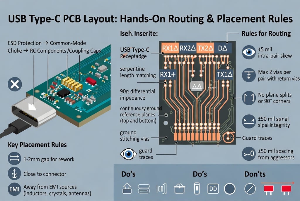
Put the connector at the board edge, positioned from the mechanical drawing. The Type-C receptacle must sit right at the board edge so cables can actually be inserted and removed. Its exact position should come from the enclosure or structural drawing — never place it by eyeball. This is precisely how Mistake #1 happens.
Separate USB inputs from USB outputs. If your design has both USB input and output ports, keep them physically apart rather than clustered together. This makes the board easier to partition and manage, and it prevents signal crosstalk between ports.
Keep the connector away from EMI sources. USB interfaces should stay clear of RF antennas (if present), crystal oscillators, and DC-DC converter inductors — all of which radiate strongly. If the USB signals sit right next to these aggressors, no amount of downstream cleanup will fully recover signal quality. Maintain at least 2–3 mm of separation, and give more if the board allows it.
Part 2: Component Placement Order — It's Not Arbitrary
Moving from the connector inward, the component order is fixed: ESD protection first, then the common-mode choke, then the RC components. Many designers don't pay attention to this sequence, but it matters. The ESD device must be the first line of defense against static discharge entering through the connector; the common-mode choke then filters common-mode noise; and the resistors and capacitors handle matching last. Reverse the order and the effectiveness of each stage is significantly degraded.
Leave a gap between the ESD device and the Type-C connector. Don't butt the ESD part right up against the receptacle — keep at least 1–2 mm of clearance. The reason is practical, not electrical: if the part is jammed against the connector shell, there's no room for a soldering iron during rework, and your repair engineers will not thank you.
Keep the ESD devices, common-mode choke, and RC components as close to the connector as possible. The farther these parts sit from the port, the more parasitic inductance and capacitance the interconnect traces introduce, and the weaker the protection becomes.
The TX/RX Coupling Capacitors Deserve Special Attention
Two points on the AC coupling capacitors for the high-speed pairs:
First, place the TX coupling capacitors near the Type-C connector. TX is the direction in which your device transmits outward, so putting the capacitor at the connector helps block high-frequency noise before it leaves the board.
Second, use approximately 100 nF — don't substitute casually. The USB 3.0 specification requires the TX-side coupling capacitance on both Host and Device to fall between 75 nF and 200 nF, and 100 nF is the most common choice. These capacitors block DC and suppress common-mode noise. Don't assume 1 µF or 0.1 µF is "close enough" and drop it in — the frequency characteristics differ, and signal integrity will suffer.
And of course, the safest reference is always your main controller's datasheet and reference design. The silicon vendor's application materials are the most reliable source for your specific chip.
Part 3: PCB Routing Rules
Type-C carries five differential pairs, and you cannot miss a single line:
RX1+ / RX1−
RX2+ / RX2−
TX1+ / TX1−
TX2+ / TX2−
D+ / D−
There's also the CC pair — not a differential pair in the strict sense, but it still deserves careful routing. A common oversight: designers remember RX/TX and D+/D− but forget that TX and RX each split into positive and negative lines across two lanes.
With the pairs identified, here are the routing rules that matter:
1. Provide a solid reference plane. Every differential signal must run adjacent to at least one continuous ground plane — adjacent planes on both sides is even better. The return path is half of your transmission line; treat it that way.
2. Length-match within each pair to ±5 mil. Intra-pair skew degrades signal quality, closes the data eye, converts differential energy into common-mode noise, and worsens EMI. Do your length compensation close to the pins, not with serpentines scattered through the middle of the route.
3. Control differential impedance to 90 Ω ±10% — and mind the continuity, not just the number. Many engineers calculate the target impedance and stop there, ignoring continuity. Continuity means: the reference plane cannot be broken, traces must never cross plane splits, trace width must not change abruptly, and corners should be arcs or 45° angles — never right angles. Any plane split crossing or reference discontinuity creates an impedance jump and signal reflections, which is exactly what high-speed signals tolerate least.
4. Be disciplined about layer changes. Every via introduces an impedance discontinuity and a reflection point. Keep vias on the USB pairs to no more than two. When a layer change is truly unavoidable, add a pair of ground return vias adjacent to the signal vias to give the return current a continuous path.
5. Shield the pairs with ground. Ground-guard the USB differential traces, keep the guard copper as continuous as possible, and stitch it with return vias at regular intervals along the route.
6. Give the pairs room — at least 50 mil from aggressors. High-speed USB signals are highly sensitive to crosstalk, and insufficient spacing is a trap you set for yourself. Keep the pairs at least 50 mil away from power nets, high-current traces, DDR, HDMI, clock lines, and other high-speed signals. If space allows, maintain spacing between the different USB pairs as well. Just as importantly, USB routing should take priority over other components and signals: route these five pairs cleanly first, then deal with everything else. A large share of "the board came back and USB doesn't work" cases trace back to USB pairs that were squeezed and contorted around everything else on the board.
Closing Thoughts
None of these rules is exotic, and none requires expensive tools — just discipline at placement and routing time. The cost asymmetry is what makes them worth internalizing: five minutes checking connector orientation, coupling capacitor values, and plane continuity before tape-out, versus a full board respin and weeks of schedule slip after.
This barely scratches the surface of USB Type-C design — the little connector holds far more knowledge than its size suggests. If there's a specific topic you'd like covered in the next installment, let us know in the comments.
SERVICES
Peakingtech © 2025. · Shenzhen, China · Privacy Policy · Terms of Service
Contact Form
Metal Parts


Peakingtech® is a registered trademark of Peakingtech Co in the United States.
COMPANY
CONTACT