
From Idea to Design
The first stage of hardware product development — from concept through engineering, enclosure design, DFM review, and the design freeze that makes manufacturing possible.
Home › How It Works › Idea to Design
Stage 1 of 4 | Pre-manufacturing phase | Typical duration: 6–14 weeks
CHAPTER 01 · HOW IT WORKS
WHY THIS STAGE MATTERS
The cheapest time to make changes is before manufacturing starts
Design decisions made on paper are free to change. The same decisions become progressively more expensive to change as a product moves from drawing to prototype to tooling to production — and most of the decisions that matter most are made in the earliest weeks.
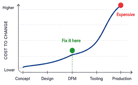
Design problems are exponentially more expensive to fix the later they're discovered
A CAD change early in design can take minutes and cost nothing. The same change after tooling is cut can require EDM rework, new fixture, or even new tools – easily adding $400 to $1,000 or more and days of delay.
This is the context for the six steps that make up the Idea to Design stage.


At design stage: 1-2 hours of engineering time
At DFM review: half a day plus minor redesign
After tooling is cut: 2 days plus $400-$1,000 for EDM rework
In production: Days of delay plus potential scrap
Fewer prototype revision cycles
THE CASE FOR DOING THIS RIGHT
Design for manufacturing is not a final checklist – it’s a lens applied throughout
Concurrent collaboration surfaces risk early, explores better options, and aligns on manufacturability, testability, and cost – leading to a more robust design that is ready for production.


A manufacturing partner involved at design stage produces a different outcome than one brought in after
Applying DFM during design helps optimize wall thickness, tolerance, draft, PCB component placement and assembly methods. It also ensures the BOM uses readily available components and realistic lead times.


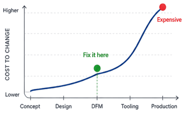
How expensive to fix a design problem at each stage of development
COST OF CHANGE CURVE
REAL COST DIFFERENCE
Integrated DFM and early collaboration typically result in 1-2 prototype revision cycles, compared to the industry-typical 3-5 cycles.
Shorter timeline
Lower total cost
Each avoided tooling modification can save 1-2 weeks. A thorough design with one prototype is consistently faster than a rushed design followed by multiple revisions.
DFM errors that reach tooling or production can add 30-60% to the budget. One tooling modification may cost $400-2,000 plus delay.


THE PROCESS
Six steps from concept to factory-ready design
Each step has a defined output and requires your approval before the next step begins. Nothing proceeds without your sign-off — at every transition, you decide.
These six steps produce a frozen design package — the output of Stage 1 and the input to Stage 2.

Discovery and Project Brief
STEP ①
2–4 days
The engagement begins with a structured discovery conversation — typically a 30–60 minute video call or detailed email exchange covering what your product does, who it's for, what the core technical requirements are, what your target unit manufacturing cost is, and what timeline you're working toward. This is not a sales call — it is an engineering intake conversation. The person on the Peakingtech side is asking the questions needed to understand what they will be asked to build, not qualifying you as a prospect.
The output of the discovery conversation is a written project brief — a document that captures everything both parties have agreed about the scope, requirements, and constraints of the project. The brief is reviewed and signed by both parties before any design work begins. It is the contract between what you described and what Peakingtech commits to designing. Changes to the brief after signing are handled as formal scope changes — they don't happen informally or by assumption.
Describe your product, its users, its core functions, and any known technical constraints or preferences. Share any existing sketches, reference products, or comparable devices. Sign the NDA before the call if file sharing is expected.


Ask the clarifying questions needed to fully understand the product scope. Identify any immediate technical or commercial concerns. Produce the written project brief and issue it for client review and signature.
STEP ②
1–2 weeks
Concept and Architecture
Based on the signed project brief, the engineering team develops a technical architecture proposal — the set of fundamental design decisions that define how the product works before any detailed design begins. This covers processor and microcontroller family selection, connectivity stack (BLE, Wi-Fi, Zigbee, LoRa, cellular — whichever applies), power management approach (battery chemistry, charging architecture, power budget), sensor and actuator selection, and the physical architecture of how the PCB and enclosure relate to each other.
For products with industrial design requirements — where the product's appearance and ergonomics are part of the specification — concept sketches are produced at this step. These are not engineering drawings; they are visual proposals showing possible form factors, proportions, and surface language. The concept document produced at this step describes how the product works and broadly what it will look like. It is the architectural blueprint before the detailed drawings begin. The client reviews and approves this document before detailed design begins — changing the architecture at Step 2 costs days; changing it at Step 4 costs weeks.
Review the architecture proposal and concept sketches. Ask questions about design decisions and request alternatives for any direction you want to explore. Confirm the industrial design direction and approve the concept document before Step 3 begins.
Develop the complete technical architecture proposal. Produce concept-level industrial design direction sketches if required by the brief. Present the proposal with clear rationale for each key decision. Revise based on client feedback until approval is obtained.
Complete the full schematic, select and verify component availability against the Shenzhen market, produce the PCB layout with signal integrity and EMC review, run the BOM against lead time and counterfeit risk databases, and prepare the complete Gerber and manufacturing package.
Review and approve component selection for any IP-sensitive, commercially critical, or preference-specific parts. Review the schematic at key milestones if you have engineering resources to do so — this is optional but valuable for clients with in-house electronics knowledge.
With the architecture approved, the electronics engineering team produces the complete electronics design. Schematic capture covers all functional blocks — power management, microcontroller and supporting circuitry, connectivity modules, sensor interfaces, indicator LEDs, user input, and programming interfaces. Component selection is validated against Shenzhen market availability and current lead times during schematic capture — not after the design is frozen. A component that is on a 16-week lead time or that has known counterfeit risk in the open market is flagged and an alternative proposed before it appears in the final BOM.
PCB layout follows schematic approval — component placement optimized for signal integrity, EMC (electromagnetic compatibility), thermal management, and assembly. The layout is reviewed against the physical constraints of the enclosure design (being developed in parallel at Step 4) to ensure component height, connector positions, and mounting hole locations are compatible with the enclosure geometry before either design is finalized. The output is a complete electronics design package — schematic, layout, BOM, and Gerber files — ready for DFM review.
Electronics Engineering
STEP ③
2–4 weeks
Produce the complete 3D CAD enclosure model in SolidWorks or Fusion 360. Run draft angle and wall thickness analysis throughout the modeling process. Produce 2D engineering drawings for all parts. Prepare the mold design brief for tooling. Document IP rating design features if applicable.
Approve the industrial design direction for the enclosure exterior — form factor, proportions, surface language, color and finish specification. Review mechanical design for any product-specific ergonomic or branding requirements. Any significant changes to the enclosure exterior after this approval are treated as scope changes.
The enclosure and mechanical design is developed directly from the PCB layout — not from a PCB outline drawing or a set of assumed dimensions, but from the actual placed PCB with component heights, connector positions, LED locations, and mounting hole locations all defined. This direct reference eliminates the most common category of enclosure fit problems: connector cutouts that don't align with the actual port positions, lid interference with components that are taller than assumed, and mounting features that conflict with PCB components on the back side of the board.
3D CAD modeling covers wall thickness and draft angle design for injection moldability, parting line and gating strategy, snap fits and assembly interfaces, mounting bosses and PCB retention features, IP rating design (TPE gasket groove or integrated seal features if an IP rating is specified), and surface finish specification for each face of the enclosure. For products with branding requirements, the locations of logos, labels, and print areas are designed into the model rather than applied as an afterthought. The output is a complete mechanical design package ready for DFM review alongside the electronics design.
Enclosure and Mechanical Design
STEP ④
2–3 weeks
Conduct the complete DFM review across electronics, enclosure, and BOM dimensions. Produce the written tiered DFM report. Propose specific, implementable solutions for every blocker. Update design files to implement approved solutions. Confirm the updated design is DFM-clean before issuing the Step 6 sign-off request.
Review the written DFM report. Ask questions about any finding you don't understand — we provide full technical explanation for every finding. Approve the resolution approach for every blocker. Acknowledge recommendations and decide which to implement. The design moves to Step 6 only when all blockers are resolved and the client has formally signed off on the DFM report.
The DFM review is a comprehensive, cross-discipline assessment of both the electronics and the enclosure design against the manufacturing processes that will produce them. It is not a generic design quality review — it is a specific review of whether these particular designs can be manufactured by these particular processes to the specified quality standard. The electronics DFM covers PCB assembly process compatibility — component placement clearances for SMT pick-and-place, pad geometry for soldering quality, fiducial marker placement for optical alignment, panelization strategy for efficient assembly, and test point accessibility for in-circuit and functional testing. The enclosure DFM covers injection molding compatibility — gate location and fill analysis, parting line cosmetic impact, ejector pin mark placement on non-cosmetic surfaces, cooling circuit design for cycle time and warpage control, and undercut analysis for any features that require side actions or lifters.
Every finding in the DFM review is classified into one of three tiers. Blockers are findings that must be resolved before manufacturing begins — they represent genuine manufacturing incompatibilities that would produce failed or non-conforming parts. Recommendations are findings that should be resolved for optimal manufacturing outcome — they represent real risks but ones where manufacturing could proceed with accepted compromise. Advisories are findings that are worth knowing but require no action — they represent design choices that have manufacturing implications the client should understand. The written DFM report separates these three tiers clearly so the client can prioritize their review and understand the relative severity of each finding.
DFM Review
3-5 days
STEP ⑤
Compile the complete frozen design package with all files at final revision. Conduct a final internal review to confirm completeness. Issue the package to the client for review. Prepare the prototype build request for the Stage 2 team.
Review the complete frozen design package — all files at final revision. Confirm that the design matches the approved project brief, the approved concept document, and all subsequent approved changes. Provide formal written sign-off authorizing the prototype build to proceed.
Design freeze is not the end of the design process — it is the formalization of the completed design into a state that can be reliably handed to manufacturing. All design files are at their final revision. All DFM blockers are resolved. All drawings are signed off. The frozen design package is complete, version-controlled, and archived. From this point forward, any change to the design — however small — is processed as a formal engineering change order (ECO) with a documented reason, an impact assessment, and an approval. This exists to protect both parties: changes after freeze have timeline and cost implications that need to be understood before they're implemented.
The frozen design package is handed to the prototype build team, beginning Stage 2 — Design to Prototype. The design freeze is the output of Stage 1 and the input to Stage 2 — the handoff point between the thinking phase and the building phase of the product journey. It represents the transition from a design that exists only in engineering files to a design that is about to exist as a physical object.
Design Freeze
1-3 days
STEP ⑥
WHAT TO PREPARE
You don't need engineering files to start
The right starting point depends on where you are in your product journey, not on having a complete design package. Here's what works at each stage — and what you can leave for later.
You have an idea
A product concept — what it does, who it's for, what problem it solves. Maybe a sketch or a description document. No engineering files.
Whichever stage you're at, the next step is the same — start a conversation and tell us what you're building.


WHAT WE DO WITH THIS
We develop the technical architecture from scratch — taking your product description and translating it into a specific set of engineering decisions: processor, connectivity, power management, sensors, enclosure form factor. The first output is a written concept document that captures how the product works, what components it uses, and what it will broadly look like. You review and approve this before any detailed design begins.
YOUR FIRST STEP
A discovery call or detailed email covering what your product does, who it's for, and what your timeline and budget constraints are. No files, no drawings, no formal spec required — a clear description of the product and a sense of what success looks like is enough to start.
HELPS TO HAVE READY
A written product description · Reference products or comparable devices · Your target retail price · Rough timeline
WHAT YOU DON'T NEED YET
Engineering files · A finalized product specification · A BOM · CAD files · Regulatory certifications plan
STAGE - IDEA
WHAT WE DO WITH THIS
We review your prototype to understand what the product does and what design decisions have already been made. We then identify what needs to change for the product to be manufacturable — component selection for production availability, PCB layout for SMT assembly, enclosure design for injection molding. Rather than starting from scratch, we use your prototype as a design reference and develop from there, carrying forward everything that works and rethinking what doesn't.
YOUR FIRST STEP
Share your prototype — either physically (ship it to our Shenzhen facility) or via detailed video and photos showing how it works and how it's assembled. A short written description of what's working well, what's not working yet, and what you know needs to change for manufacturing is also valuable. If you have any existing schematic or code, share that too — even if it's rough.
HELPS TO HAVE READY
Photos or video of the prototype in operation · Any existing schematic (rough is fine) · List of known issues or limitations · Your target production cost per unit
WHAT YOU DON'T NEED YET
Production-ready PCB layout · Injection mold CAD · Final BOM · Regulatory testing
A working prototype — breadboarded, built on a development kit, or 3D printed. It demonstrates the product function but isn't manufactured.
You have a working prototype
STAGE - PROTOTYPE


WHAT WE DO WITH THIS
We conduct a comprehensive DFM review of your existing files against the specific manufacturing processes that will produce your product — SMT assembly for the PCB, injection molding for the enclosure, and BOM availability for the component selection. The review produces a tiered report: blockers that must be resolved before manufacturing, recommendations that should be resolved for optimal outcome, and advisories that are worth knowing but require no action. We then either implement the changes ourselves or provide detailed guidance for your own engineering team.
YOUR FIRST STEP
Share your Gerber files, STEP file (for enclosure CAD), and BOM. An NDA is signed before we review any files — you can request the NDA before sending anything. Along with the files, share any known design constraints or requirements: IP rating, specific certifications, target unit cost, any components you've already committed to sourcing from specific suppliers.
HELPS TO HAVE READY
Gerber files and BOM · STEP file for enclosure (if applicable) · List of committed components or suppliers · Target unit manufacturing cost
WHAT YOU DON'T NEED YET
A manufacturing-ready design · Completed tooling plans · Regulatory certifications · A production schedule
A schematic, PCB layout, or 3D CAD file — or all three. The design is done or nearly done but hasn't been through a manufacturing DFM review.
You have engineering files
STAGE - FILES


Not sure which stage describes you?
Most hardware founders fall somewhere between these three stages — you have more than an idea but less than complete files, or you have complete electronics files but no enclosure design yet. That's fine.
The simplest rule: contact us when you have enough clarity to describe what your product does in two to three sentences and tell us who it's for. That's the minimum starting point for a productive first conversation.
If you're between idea and prototype: — Start with Card 1 (Idea stage). A concept that hasn't been built yet is still a valid starting point.
If you're between prototype and files: — Your working prototype is closer to Card 2. The existing prototype is the starting point for the engineering design, not a detour around it.
If you have some files but not a complete package: — Share what you have. A partial schematic and a rough enclosure sketch is more than enough to start a DFM conversation. We'll identify what's missing.
What to expect on time and budget
Indicative ranges based on typical hardware product complexity. Exact timelines and costs are confirmed in the project brief at Step 1 — before any design work begins.
TIMELINE & COST
Note 1: Design stage cost is separate from prototype build, tooling, and production costs — those belong to Stages 2 and 3.
Note 2: The project brief at Step 1 produces a fixed-price quote for the complete design stage — no hidden costs after agreement.
Note 3: NPI projects qualify for phased payment — 50% at project brief, 25% at concept approval, 25% at design freeze.
Stage 1 timeline breakdown
① Discovery
2-4 days
② Concept & Architecture
1-2 weeks
③ Electronics Engineering
④ Enclosure Design
⑤ DFM Review
⑥ Design Freeze
2-4 weeks
2-4 weeks
3-5 days
1-2 days
Total: 6-14 weeks concept to design freeze
Shorter end: simple product, clear breif
Longer end: complex product, more revision rounds
Stage 1 cost framework
$1,000-$3,000
design stage total
TIER 01
Simple Product
Simple PCB, standard enclosure, clear brief
TIER 02
Medium Complexity
Custom electronics enclosure, moderate engineering work
$3,000-$5,000
design stage total
TIER 03
High Complexity
Multiple subsystems, advanced constraints, heavy iteration
$5,000-$10,000
design stage total
Ready to take your idea to design?
Tell us what you're building and where you are in the process — we'll outline the right first step for your situation, at no charge.
START STAGE ONE
No commitment required · Response within 24 hours · NDA available before any file sharing
What happens next
1.We read your message
A member of the product development team reads your submission — not a sales contact, not an automated response. Someone who works with NPI projects.
2.We respond with a recommendation
Within 24 hours: a specific recommendation on the right first step for your situation — whether that's a discovery call, a DFM review, or a prototype assessment. No generic sales response.
3.We have a conversation
A 30–45 minute call covering your product, your timeline, and what Stage 1 looks like for your specific situation. No commitment required at any point before the project brief is signed.
Stage 1 output (design package) is the input to Stage 2. Once design is frozen, we begin building.
See Stage 2: Design to Prototype →


SERVICES
Peakingtech © 2025. · Shenzhen, China · Privacy Policy · Terms of Service
Contact Form
Metal Parts


Peakingtech® is a registered trademark of Peakingtech Co in the United States.
COMPANY
CONTACT