
From Design to Prototype
The second stage of hardware product development — from frozen design through PCBA assembly, enclosure first shots, functional testing, and the prototype approval that authorizes production.
Home › How It Works › Design to Prototype
Stage 2 of 4 | First physical build phase | Typical duration: 4–8 weeks
CHAPTER 02 · HOW IT WORKS
WHAT THIS STAGE IS
A prototype is how you discover what needs to change — not proof that nothing does
Every first prototype reveals something. The question is not whether your prototype will need changes — it's whether those changes are minor refinements or significant revisions, and whether you have a plan for addressing them efficiently.
A prototype has three specific jobs — and a finished product is not one of them
A hardware prototype serves three key purposes: functional validation (electronics, firmware, sensors, connectivity), mechanical validation (enclosure fit, alignments, assembly), and aesthetic validation (look, feel, finish). One that passes all three is production-authorized. Others identify design issues before they reach production.
With that framing in place — here is exactly what happens during the prototype stage.


PURPOSE
Most first PCBA builds power on and function
WHAT A PROTOTYPE ACTUALLY IS
Most first prototypes work — and most first prototypes also reveal something
The prototype stage produces a complete evaluation package — functional and dimensional reports, inspection photos, fit checks, and an enumerated list of changes — which drives the production authorization decision. Revisions use a clear brief to manage fixes; authorized prototypes join the technical file. Both outcomes are documented and valuable.


The prototype stage ends with a document, not just a product
The first PCBA typically powers on, runs firmware, and demonstrates core functions, while revealing normal refinements like power adjustments, RF layout issues, or inaccessible test points—caught cheaply before production. The first enclosure shot meets critical dimensions but often needs minor tooling tweaks for finish or sink marks, resolved quickly and inexpensively.


What a prototype is — and what it is not
PROTOTYPE VS PRODUCTION UNIT
The majority of PCBA prototypes built from a thoroughly DFM-reviewed design power on successfully and demonstrate core product functions on the first build. Firmware issues are common - hardware issues requiring a PCB revision are less common and typically minor when they occur.
——————
At Peakingtech: approximately 80% of first PCBA prototype builds proceed to functional testing without assembly rework. Of those that require rework, the majority are resolved with component substitution rather than PCB redesign.
First enclosure shots are typically dimensionally correct
Most products need one revision cycle or fewer


The distinction between prototype and production unit is not about quality — it's about purpose. A production-authorized prototype is the same quality as a production unit. The difference is the documentation that validates the design before production begins.
No new design issues. Production issues (process variation, yield) managed by QC.
Validate that the design works as intended. Discover what needs to change before production.
PROTOTYPE
PRODUCTION UNIT
ISSUES
Issues expected and planned for. Every issue is documented, classified, and addressed.
Produce units to a confirmed specification for commercial delivery.
OUTPUT
Physical sample units + prototype evaluation package (test reports, inspection reports, revision brief).
Commercial units meeting the confirmed product specification.
ACCEPTED IF
All validation areas assessed. Issues documented and classified. Production authorized.
Meets confirmed product specification. Passes incoming QC per acceptance criteria.
NEXT STEP
Production authorization or revision brief (build revised prototype, repeat evaluation).
Shipment to customer or fulfillment center.
The majority of first injection mold shots are dimensionally within specification for the critical features - connector cutout positions, PCB mounting hole locations, and external envelope dimensions. Surface finish variations and minor cosmetic issues on non-critical surfaces are more common and are addressed with tooling adjustments rather than new tooling.
——————
At Peakingtech: approximately 90% of first enclosure shots achieve a successful PCB fit check. Tooling adjustments (not replacements) resolve the majority of first-shot cosmetic issues within 2-5 days.
Hardware products that go through thorough design DFM review at Stage 1 typically complete the prototype stage in one build cycle (no revision) or one revision cycle. Products that enter the prototype stage without DFM review average more revision cycles because design problems that DFM would have caught are discovered during testing instead.
——————
At Peakingtech: products completing Stage 1 DFM review average 1.2 prototype build cycles before production authorization. Products entering prototype without prior DFM review average 2.4 cycles. The DFM investment in Stage 1 approximately halves the prototype stage duration.
THE PROCESS
Five steps from frozen design to approved prototype
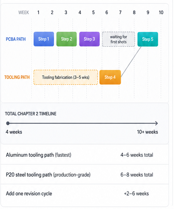
Each step has a defined output and a client review point. PCBA assembly and enclosure tooling run concurrently — the total timeline is shorter than the sum of the individual step durations.
These five steps produce either a production authorization or a revision brief — both are defined outcomes with clear next steps.

See how prototype revision cycles work ↓
Build Preparation and Component Sourcing
STEP ①
3–7 days
The prototype build begins with the frozen design package from Stage 1 — the complete electronics files, mechanical files, and signed client approval document. The build team reviews the package for completeness: all Gerber layers present and correctly named, all BOM part numbers confirmed, STEP file and 2D drawings for the enclosure design complete. If any element of the package is incomplete, it is resolved before the build schedule is committed.
Components are sourced from Shenzhen's authorized distributor network — every BOM line item checked for availability and lead time before the build is scheduled. Bare PCBs are ordered from a Shenzhen PCB fabricator (typically 2–5 business days turnaround for standard stack-up, 24–48 hours for expedited). The SMT stencil is produced simultaneously with the PCB order. A build traveler — the internal document that records every process step, inspection result, and decision point for this specific build — is prepared before assembly begins.
Confirm any consignment components being supplied directly — their part numbers, quantities, and expected delivery date to our Shenzhen facility. Review and confirm the final BOM if any line items were substituted due to availability at sourcing stage.


Review the frozen design package for completeness. Source all BOM components from authorized distributors. Order bare PCBs and stencil. Confirm build schedule. Produce the build traveler. Notify client of any BOM substitutions made for availability reasons.
STEP ②
2–5 days
PCBA Assembly
SMT assembly begins with solder paste application through the stencil produced at Step 1 — a 1:1 aperture-mapped stencil that deposits the correct paste volume on each PCB pad. Component placement follows using the pick-and-place program generated from the Gerber centroid data, placing components at the rates and sequences optimized for this specific PCB layout. Reflow soldering in a profiled oven with a temperature ramp calibrated to the specific solder alloy and board thickness produces the final solder joints. Through-hole components (if the BOM includes any) are assembled after reflow — by hand for prototypes, by selective solder or wave for production.
Automated optical inspection (AOI) follows reflow — a camera-based inspection system that checks every placed component against the pick-and-place program, verifying placement, polarity, and the absence of solder bridges or missing components. For boards containing BGA or QFN packages where the solder joints are not visible from above, X-ray inspection provides solder joint quality verification below the package body. The final inspection is a manual IPC-A-610 Class 2 review — a technician inspects each board against the IPC visual acceptance criteria for solder joint quality, lead protrusion, component seating, and workmanship. All three inspections are documented in the assembly report.
No action required during PCBA assembly. Build progress updates provided at two points — build start confirmation and build completion notification. Review the assembly report and first article photographs when they are issued at step completion.
Execute SMT assembly per the build traveler sequence. Run AOI after reflow, document all findings and rework performed. Execute X-ray inspection for BGA and QFN packages. Perform manual IPC-A-610 Class 2 inspection of all boards. Compile the assembly report with inspection results, process photographs, and rework log.
Load firmware to all boards. Execute power-on verification for each board. Execute the approved functional test specification for each board. Document all results — pass, fail, and conditional pass. Produce failure reports for all failing tests including initial root cause hypothesis. Compile the first article functional test report and issue to client.
Review and approve the functional test specification before testing begins — this is the document that defines what "passing" means for your product. Review the first article functional test report when issued. For any failing tests: confirm the failure is reproducible, review the proposed root cause analysis, and approve the investigation approach before hardware investigation begins.
Firmware is loaded to each assembled PCBA using the programming interface designed into the PCB at Stage 1 Step 3 — a dedicated programming header, a JTAG interface, or an OTA (over-the-air) update path if the connectivity stack supports it. The programming process itself confirms that the microcontroller is communicating with the programmer — a basic but important first test of the power supply, crystal oscillator, and microcontroller function. Each successfully programmed board is then powered on for the first time and observed for any anomalies — unexpected current consumption, incorrect LED states, or unexpected resets — before structured testing begins.
Structured functional testing follows a test specification produced from the project brief — each functional requirement stated in the brief ("the sensor shall read temperature to ±0.5°C accuracy," "the BLE connection shall establish within 3 seconds of power-on") is tested with a defined procedure and the result recorded as pass, fail, or conditional pass. For prototype builds, the test specification is reviewed and agreed with the client before testing begins. Any failing test generates a failure report — the specific test that failed, the observed behaviour, the expected behaviour, and the initial hypothesis for root cause. The first article functional test report collects all pass/fail results, all failure reports, and any observations about board behaviour that don't constitute test failures but are worth noting.
Functional Testing and Firmware Loading
STEP ③
2–5 days
Execute first shots per the tooling process setup documentation. Perform dimensional inspection of all critical features against 2D drawings. Execute fit check with assembled PCBA. Document all dimensional results, deviations, and cosmetic observations. Produce the first shot inspection report with photographs. Make tooling adjustment recommendations for any out-of-tolerance features. Execute approved tooling adjustments and confirm with second shots if required.
Review the dimensional inspection report and fit check results when issued. Evaluate the prototype enclosure aesthetically — surface finish, parting line appearance, colour accuracy. Provide written feedback on cosmetic acceptance within the agreed review period. Approve or reject the first shots — approval authorises the assembly of complete functional prototypes at Step 5; rejection triggers a documented tooling adjustment.
The injection mold tooling fabricated concurrently with Steps 1–3 is now ready for first shots. The mold is mounted in the injection molding machine, process parameters are set (melt temperature, injection speed, pack pressure, cooling time), and the first parts are shot. For prototype builds using aluminum rapid tooling, first shots typically happen within 24 hours of tool completion — aluminum tools are faster to set up and debug than steel production tools. For production-path builds using P20 steel tooling, first shots follow a more structured qualification process with initial fill studies before full-cavity production.
First shots are inspected dimensionally against the 2D engineering drawings from Stage 1 Step 4 — every critical dimension checked with calibrated instruments, results recorded against the drawing tolerances. Critical dimensions include connector cutout positions (checked against the PCB layout data), PCB mounting hole positions, lid-to-base mating surface flatness, and any features that affect the product's IP rating or assembly function. The fit check follows dimensional inspection — a fully assembled PCBA is placed into the enclosure base, the connectors are verified to align with their cutouts, the mounting bosses engage with the PCB holes, the lid mates with the base, and the complete assembly is functionally operated. Any dimensional deviations are documented with the measured value, the drawing nominal, and the tolerance. A tooling adjustment recommendation is made for any deviation outside tolerance.
Enclosure First Shots and Fit Check
STEP ④
3–5 days after tooling
Compile the complete prototype evaluation package from all step outputs. Produce the evaluation meeting agenda with specific discussion items for each outstanding issue. Facilitate the evaluation meeting. Issue the production authorization document or revision brief based on the evaluation outcome. For conditional authorization, document each conditional item with its implementation commitment and verification method.
Attend the prototype evaluation meeting — typically a 60–90 minute video call covering all build results. Review all documentation in advance of the meeting. Make the production authorization decision: full authorization, conditional authorization with documented items, or request for a revision brief. If a revision brief is required, review and approve the revision brief content before revision build scheduling begins.
All prototype build outputs are now complete — the assembled PCBA with functional test results, the enclosure first shots with dimensional inspection and fit check results, and the complete build traveler documenting every process step. The prototype evaluation meeting brings all of these outputs together for a structured review with the client. The meeting covers the functional test results (each test result with context from the test specification), the first shot results (dimensional inspection and fit check, with photographs), any outstanding observations from the build (component behaviour notes, assembly sequence observations, tooling notes), and a proposed disposition for each outstanding item — implement before production, monitor through production, or accept as-is.
The prototype evaluation has three possible outcomes. The first is full production authorization — all functional tests pass, first shots are within dimensional tolerance, fit check is successful, and the client is satisfied with the cosmetic result. The prototype is approved as-is and Stage 3 begins. The second is conditional production authorization — the prototype is functionally and dimensionally acceptable but with documented minor items (a cosmetic improvement, a non-critical component value tweak, a label position adjustment) that will be implemented at production without requiring a new prototype build. The third is a revision brief — one or more items identified in the evaluation require resolution and verification before production authorization can be granted. A revision brief defines each item precisely, proposes a resolution, and specifies the test or inspection that will confirm the resolution before authorization.
Prototype Evaluation and Approval
3-7 days
STEP ⑤
REVISION CYCLES
How many prototype iterations are normal — and what drives them
Most hardware products need between zero and two prototype revision cycles before production authorization. Understanding what type of revision you're dealing with — electronics, enclosure, or integration — determines the timeline, cost, and resolution path.
A hardware change is needed to the PCB design
An electronics revision is triggered when functional testing at Step 3 reveals a hardware problem that cannot be resolved through firmware changes alone — a power supply that doesn't regulate correctly at load extremes, an RF layout that fails to meet the antenna specification, a signal integrity problem affecting communication reliability. Electronics revisions require a PCB design change, a new PCB fabrication and assembly, and a new round of functional testing.
With a clear picture of revision cycles, the next step is understanding total timeline and cost.
WHAT CAUSES IT
Power supply instability at load extremes
RF layout affecting antenna performance
Signal integrity on high-speed interfaces
Component value requiring adjustment for thermal or frequency variation
ESD protection insufficient for the application
RESOLUTION PATH
Schematic updated for the identified issue. PCB layout revised accordingly. New bare PCBs ordered and assembled. BOM updated if component changes are required. Functional testing repeated for the affected functions and a regression test run to confirm no new issues were introduced.
TIMELINE AND COST
PCB revision and new assembly: 1–2 weeks additional timeline. Cost: typically $800–$2,500 for a single-board electronics revision build including new bare boards, assembly, and testing. Component substitutions that don't require PCB layout changes are resolved without a revision build.
ELECTRONICS REVISION
WHAT CAUSE IT
Dimensional deviation outside tolerance requiring tooling adjustment
Warpage on large flat panels (cooling design or material issue)
Sink marks on cosmetic surfaces adjacent to thick features
Parting line position affecting cosmetic quality
Connector cutout position off-nominal requiring tooling metal removal
RESOLUTION PATH
For tooling adjustment: identify the specific dimension deviation and direction, machine the mold steel to correct the deviation, shoot second shots to verify the correction. For design revision: update the 3D CAD model, revise 2D drawings, update the mold design brief, machine a new cavity or use an insert to implement the design change, first shots from the revised tool.
TIMELINE AND COST
Tooling adjustment: 2–5 days additional timeline, $200–$800 cost. Design revision with new cavity: 2–4 weeks additional timeline, $1,500–$5,000 depending on the scope of the change. Tooling adjustment is by far the more common resolution — design revisions are relatively rare for products that went through thorough DFM review.
An enclosure revision is triggered when first shots at Step 4 reveal dimensional deviations outside tolerance, cosmetic issues that don't meet the agreed acceptance criteria, or fit check failures that can't be resolved by tooling adjustment alone and require a design change to the 3D CAD model. Most first-shot issues are resolved by tooling adjustment — modifying the mold steel without redesigning the part.
A tooling adjustment or design change is needed for the enclosure
ENCLOSURE REVISION
WHAT CAUSE IT
Component placement close to PCB edge creating enclosure clearance conflict
Connector body protrusion greater than enclosure cutout depth allows
PCB flex or warpage under heat creating interference with enclosure features
LED position shift after reflow creating misalignment with enclosure window
Mounting boss height insufficient for actual component height on PCB back side
RESOLUTION PATH
PCB layout updated to resolve the component placement conflict. Enclosure 3D CAD updated to match the revised PCB layout. 2D drawings revised. Tooling modified or new tooling produced as required. New PCBA assembled. New first shots from modified tooling. Full fit check repeated. Both changes implemented simultaneously — changing one without the other does not resolve an integration conflict.
TIMELINE AND COST
Integration revision adds 3–6 weeks to the total prototype timeline. Cost: $2,500–$8,000 depending on the scope of changes to both PCB and enclosure. Integration revisions are the most commercially significant outcome of a first prototype build — they are also the revision type most effectively prevented by thorough Stage 1 DFM review, which specifically targets the PCB/enclosure interface.
An integration revision is triggered when the fit check at Step 4 reveals an incompatibility between the PCB and the enclosure that cannot be resolved by adjusting either alone. The most common scenario: a PCB component placed close to the board edge creates a clearance conflict with the enclosure wall that requires both the PCB layout to move the component and the enclosure design to adjust the wall relief feature simultaneously.
A coordinated change is needed to both the PCB and the enclosure
INTEGRATION REVISION




What reduces prototype revision probability?
Actions taken at Stage 1 and during the prototype build that most significantly reduce the frequency and severity of revision cycles.
AT STAGE 1 - DESIGN STAGE
Thorough DFM review
Component availability verification
Concurrent PCB and enclosure design
Connector position confirmed from actual layout data
AT PROTOTYPE STAGE
Approve the functional test specification early
Review assembly results before firmware loading
Review first-shot photos before fit check
Respond quickly at approval gates
What to expect on time and budget for Stage 2
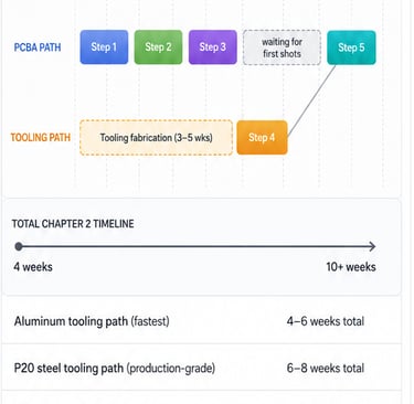
The Stage 2 timeline is not the sum of the individual step durations — PCBA assembly and enclosure tooling fabrication run concurrently. The total duration depends on which path is longer and how many revision cycles are needed.
TIMELINE & COST
Note 1: Prototype build cost is separate from Stage 1 design stage cost and Stage 3 production tooling cost — these are three distinct budget line items.
Note 2: P20 steel production tooling cost (when used at prototype stage) is a one-time cost — the same tool is used for production. It does not recur at Stage 3.
Note 3: A revision build adds approximately 50–70% of the original build cost — not the full original cost, because BOM sourcing is faster the second time and the test specification already exists.
Note 4: PCBA build cost and enclosure tooling cost are quoted as separate line items — you see both components of the total before committing.
Note 5: Functional testing and DFM compliance review are included in all prototype build quotes — not charged as additional services.
Stage 2 timeline — concurrent paths
Stage 2 cost framework
$1,000-$3,000
prototype build total
TIER 01
Simple Product
Simple PCB, standard two-part enclosure, no IP rating, aluminum rapid tooling, no prior DFM issues expected
TIER 02
Medium Complexity
Multi-feature PCB, custom enclosure with IP rating, P20 steel tooling, wireless connectivity testing, one revision cycle allowed for
$3,000-$5,000
prototype build total
TIER 03
High Complexity
Multi-board system, complex enclosure, full production tooling path, multiple certification-required tests, potential for multiple revision cycles
$5,000-$10,000
prototype build total
Ready to build your first prototype?
Tell us about your design and where you are in Chapter 2 — we'll confirm the build approach, timeline, and cost within 48 hours.
START STAGE TWO
NDA before file sharing · Fixed-price prototype quotes · Response within 48 hours
What happens next
1.We review your design files
A build engineer reviews your frozen design package — Gerbers, BOM, STEP file, and drawings. If files aren't ready yet, we respond with a preliminary estimate and a request for files when available.
2.We produce a build quote
Within 48 hours: a fixed-price quote for the prototype build covering PCBA assembly, tooling cost (if applicable), functional testing, and inspection. BOM pricing provided as a line-by-line breakdown — you see every component cost.
3.We confirm the build schedule
Once the quote is approved and files are confirmed, we confirm the build schedule — component sourcing starts, tooling order is placed, and the build traveler is issued. Build start is typically within 5–10 business days of quote approval for standard BOM compositions.
Next Stage:
Prototype to Production →


SERVICES
Peakingtech © 2025. · Shenzhen, China · Privacy Policy · Terms of Service
Contact Form
Metal Parts


Peakingtech® is a registered trademark of Peakingtech Co in the United States.
COMPANY
CONTACT