
How to Choose the Right Copper Weight for Your PCB: A Practical Guide
One of the most common questions we hear during PCB prototyping is: "Is thicker copper always better?" The short answer is no. Copper thickness is a trade-off, not a spec you max out.
Peakingtech Engineering Team
7/10/20268 min read
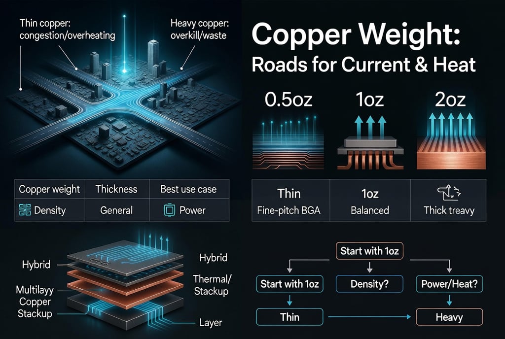
If you think of a PCB as a city, then the copper traces are its road network — the highways that carry current and signals from one point to another. Make the roads too narrow and you get congestion (overheating, voltage drop, even trace failure). Make them too wide and you're paying for asphalt nobody drives on. That, in a nutshell, is the copper weight decision every hardware designer faces.
One of the most common questions we hear during PCB prototyping is: "Is thicker copper always better?"
The short answer is no. Copper thickness is a trade-off, not a spec you max out. The right choice depends on how much current your board needs to carry, how it dissipates heat, how fine your routing needs to be, and — inevitably — how much you're willing to pay. In this guide, we'll walk through how copper weight is measured, what the common options are, where each one fits, and how to make the call for your own design.
What "Copper Weight" Actually Means
In the PCB industry, copper thickness is expressed in ounces (oz). It sounds odd at first — why measure thickness in a unit of weight? The convention comes from how copper foil is specified: 1 oz means one ounce of copper rolled out evenly over one square foot of area, which works out to a thickness of approximately 35 µm (about 1.4 mils).
Once you know the conversion, the rest of the scale is easy to read:
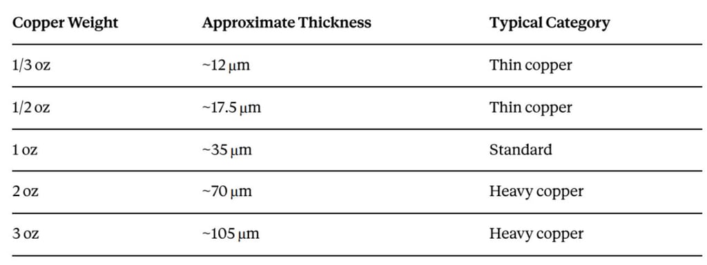
These five weights — 1/3 oz, 1/2 oz, 1 oz, 2 oz, and 3 oz — cover the vast majority of boards manufactured today. Heavier options exist for specialized power applications, but for most product designs, your decision will land somewhere in this range.
Why Thicker Isn't Automatically Better
It's tempting to treat copper thickness like a safety margin: more copper, more current capacity, more headroom. And it's true that a thicker trace carries more current and spreads heat better. But every increase in copper weight brings real costs on the manufacturing side:
Etching gets harder. PCB traces are formed by etching away unwanted copper. The thicker the foil, the longer the etchant has to work, and the more it undercuts the trace sidewalls. This limits how fine your traces and spacing can be. A fab that comfortably produces 3.5 mil traces on 1/2 oz copper may need 6–8 mils or more on 2 oz copper.
Cost goes up. Copper is a commodity material, and thicker foil means more of it. Heavy copper boards also require adjusted lamination and etching processes, which adds to the fabrication price — especially at prototype quantities.
Impedance control gets trickier. For high-speed designs, trace geometry directly determines impedance. Thicker copper changes the cross-section of every trace, and the wider etch tolerances of heavy copper make it harder to hit tight impedance targets consistently.
Soldering behavior changes. Thick copper planes are excellent heat sinks — which is exactly what you don't want during reflow. Heavy copper boards can pull heat away from solder joints during SMT assembly, requiring adjusted thermal profiles to avoid cold joints.
So the real question isn't "how much copper can I get?" It's "how much copper does this design actually need?" That comes down to four factors: current, heat dissipation, cost, and process requirements.
Thin Copper (1/2 oz and Below): Built for Density
Thin copper — 1/2 oz, 1/3 oz, and below — is the choice when routing density matters more than raw current capacity.
Because thinner foil etches faster and more precisely, fabricators can produce finer traces and tighter spacing on it. That makes thin copper the natural fit for:
Communication equipment, where boards are packed with high-pin-count devices and controlled-impedance routing
High-integration IC applications, including fine-pitch BGAs where escape routing demands very narrow traces
HDI designs in general, where every fraction of a millimeter of routing channel counts
The advantage is simple: the lines can be made finer, which gives layout engineers much more room to work in dense areas. If your design revolves around a 0.4 mm pitch BGA or dense differential pair routing, thin copper on the outer or signal layers is often not just preferable — it's necessary.
The trade-off, of course, is current capacity. A thin trace can only carry so much before it heats up, so power delivery on thin-copper boards typically relies on wider pours, more vias, and careful plane design.
1 oz Copper: The Industry Default for a Reason
If there's one number to remember from this article, it's this: 1 oz (~35 µm) is the most common copper weight in PCB prototyping and production, and it's the default at virtually every fab house.
Why has 1 oz become the standard? Because it sits at the sweet spot between three competing demands:
Electrical performance — enough cross-section to carry the currents typical of consumer electronics, industrial controls, and general PCBA products without excessive trace widths
Process stability — thick enough to survive handling and plating with good yield, thin enough to etch cleanly with reliable tolerances
Cost control — standard material stocked by every laminate supplier and fab, with no process surcharges
For most consumer electronics, industrial control boards, and general-purpose PCBA work, 1 oz simply works. Unless your design has a specific reason to deviate — extreme density on one end, high current on the other — 1 oz is the sensible starting point, and you should require a justification to move away from it rather than a justification to stay.
Heavy Copper (2 oz and Above): Built for Power
Boards with 2 oz copper and above fall into the heavy copper category, and they exist for one reason: moving serious current and serious heat.
Doubling copper thickness roughly doubles the current a trace of the same width can carry at the same temperature rise. It also dramatically improves the board's ability to spread and dissipate heat, since the copper itself acts as a thermal conductor pulling heat away from hot components.
That's why heavy copper is the standard choice in:
Power modules — DC-DC converters, inverters, and power supplies where traces routinely carry tens of amps
New energy vehicles — battery management systems, motor controllers, and charging electronics
Industrial power equipment — motor drives, welding equipment, and high-power industrial supplies
High-power devices generally, where thermal management is a first-order design constraint
The trade-offs we covered earlier apply in full here: coarser trace geometry, higher fabrication cost, and more demanding assembly. Heavy copper is a deliberate engineering choice for power-dense designs — not an upgrade you sprinkle onto a board "just in case."
One practical note: you don't have to use the same copper weight on every layer. A common approach in power designs is a hybrid stackup — heavy copper on the power layers, standard or thin copper on the signal layers — giving you current capacity where you need it and routing density where you need that.
How Copper Weight Ripples Through Design and Assembly
Copper thickness isn't a parameter you can pick in isolation. During both PCB fabrication and downstream SMT assembly, it interacts with almost everything else:
Trace width design. Your minimum trace width and spacing rules depend directly on copper weight. Current-carrying calculations (IPC-2152 is the modern reference) take thickness as a core input — the same 10 A trace needs to be roughly twice as wide on 1 oz as on 2 oz.
Etching precision. As discussed, thicker copper means larger etch tolerances. If your design has both fine-pitch routing and high-current paths, that tension needs to be resolved early — often through the layer stackup rather than a single compromise weight.
Impedance control. Controlled-impedance traces are calculated from a specific cross-section. Change the copper weight and the target widths change with it. Always lock in copper weight before finalizing impedance-controlled routing.
Soldering quality. During reflow, heavy copper layers sink heat away from joints. Fabs and assembly houses compensate with adjusted thermal profiles, but the design side can help too — thermal relief connections on pads tied to large copper areas make a real difference in joint quality.
This is why copper weight belongs in the conversation at the design stage, not as an afterthought at the ordering stage. When our engineering team reviews a new project, matching copper thickness to the actual current-carrying requirements is one of the first things we check — it's far cheaper to get right in DFM review than to discover in testing that a power trace runs hot.
A Simple Decision Framework
If you're staring at the copper weight dropdown on a fab order form, here's a quick way to think through it:
Start with 1 oz as your baseline. It's the default for a reason, and it's right for most designs.
Go thinner (1/2 oz or below) only if routing density demands it — fine-pitch BGAs, dense communication boards, HDI structures.
Go heavier (2 oz+) only if current or heat demands it — run the numbers on your highest-current traces using IPC-2152, and check your thermal budget.
Consider a mixed stackup if your design needs both density and power. Different weights on different layers is a standard, well-supported approach.
Talk to your fabricator early. Copper weight affects minimum trace/space capability, impedance calculations, cost, and lead time. A five-minute conversation during design review beats a respin.
Frequently Asked Questions
Q1: Is thicker copper always better for PCB performance?
Not necessarily. While thicker copper carries more current and dissipates heat better, it also increases fabrication difficulty and cost, limits how fine your traces can be, and complicates impedance control and soldering. The right copper weight is the one matched to your actual application requirements.
Q2: Why is 1 oz the most common copper weight?
Because it strikes the best overall balance between conductivity, process stability, and cost control. It handles the current levels typical of most electronic products, etches cleanly with reliable tolerances, and carries no cost premium — which is why it suits the majority of consumer, industrial, and general PCBA designs.
Q3: Where is heavy copper mainly used?
Heavy copper (2 oz and above) is used in applications with high current, high power, and demanding heat dissipation — primarily new energy vehicles, power modules, industrial power supplies, and other high-power equipment.
Q4: Can I use different copper weights on different layers of the same board?
Yes, and it's common practice. Hybrid stackups — for example, 2 oz on power layers and 1/2 oz or 1 oz on signal layers — let you combine high current capacity with fine routing density on a single board.
Q5: How does copper weight affect SMT assembly?
Thicker copper acts as a heat sink during reflow soldering, pulling heat away from joints. Assembly houses compensate with adjusted thermal profiles, and designers can help by using thermal relief connections on pads attached to large copper areas.
Final Thoughts
Copper weight is one of those quiet parameters that touches nearly every aspect of a PCB — electrical performance, thermal behavior, routing density, manufacturability, and cost. There's no universally "best" thickness, only the thickness that fits your design.
For most products, 1 oz is the answer. For dense, high-speed communication boards, thin copper opens up routing room that standard copper can't offer. For power electronics, heavy copper is what keeps traces cool and boards reliable. The key is making the choice deliberately, early, and in conversation with your fabricator.
We've been manufacturing PCBs for over a decade, and along the way we regularly share practical knowledge on PCB prototyping, PCBA, SMT assembly, and integrated circuit applications. If you're unsure which copper weight fits your next project, send us your design requirements — our engineering team reviews copper thickness against current-carrying needs as a standard part of every project evaluation.
SERVICES
Peakingtech © 2025. · Shenzhen, China · Privacy Policy · Terms of Service
Contact Form
Metal Parts


Peakingtech® is a registered trademark of Peakingtech Co in the United States.
COMPANY
CONTACT