PCB Surface Finishes: The Decision That Determines Whether Your Board Survives Mass Production
Most people ordering PCBs focus on two things: price and lead time. Surface finish? Just pick whatever's on the quote.
Peakingtech Engineering Team
7/10/20266 min read
Most people ordering PCBs focus on two things: price and lead time. Surface finish? Just pick whatever's on the quote.
Here's the truth after 10 years of engineering and tearing down boards: when a board "won't solder," oxidizes fast, or keeps coming back for rework, the root cause is often not the assembly line — it's a surface finish that was wrong from day one.
This guide is written for technicians, engineers, and project decision-makers. One pass through the major finishes: what each one does well, where it bites, and when to use it.
First, Understand What a Surface Finish Actually Does
Protects the copper. Bare copper starts oxidizing within hours of exposure, and oxidized copper won't take solder.
Enables solderability. Soldering is the formation of an intermetallic compound (IMC) between tin and copper — the finish defines the quality of that interface.
Defines your process window. How many reflow cycles the board can survive, how long it can sit in storage, whether it can go through wave soldering — all set by the finish.
Affects electrical and mechanical performance. High-frequency signal loss, contact resistance, mating cycles, wire bonding — all directly tied to the finish.
In short: a surface finish is not a cosmetic option. It's part of your reliability design.
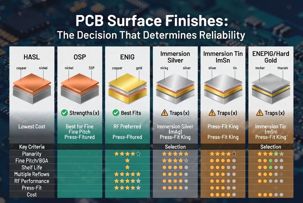
The Six Mainstream Finishes: Strengths, Traps, and Where They Belong
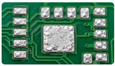
1. HASL — Hot Air Solder Leveling (Leaded / Lead-Free)
Strengths
Lowest cost, most mature process — virtually every board shop runs it
Excellent solderability; the surface is solder, so wetting is fast
Long shelf life (12+ months), tolerates multiple reflow cycles
Forgiving for rework — the least stressful option on a production line
Traps
Poor planarity. Solder thickness varies wildly across pads (1–40 µm), leaving fine-pitch pads uneven
Avoid below 0.5 mm pitch, BGA, and QFN. Bridging and open joints become a "mandatory course"
Thermal shock: the board passes through a 260 °C+ solder bath — thin boards warp
Leaded HASL fails RoHS; lead-free HASL runs even hotter and demands better laminates
Unsuitable for press-fit holes and aluminum-core boards
Best fit
Mid-to-low density consumer and industrial boards
Component pitch ≥ 0.65 mm, no BGA or only coarse-pitch BGA
High-volume, cost-driven projects
2. OSP — Organic Solderability Preservative
Strengths
Low cost (on par with or below HASL)
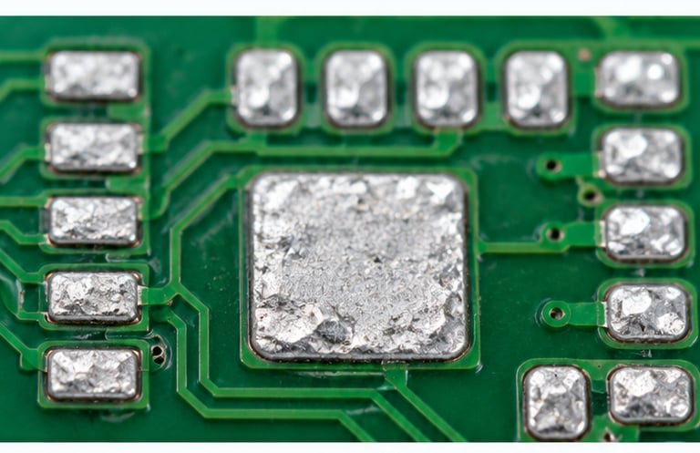
Perfectly flat — the copper itself is the soldering surface, ideal for fine pitch
Environmentally friendly process, no metal deposition
The joint is a clean tin-copper IMC — joint reliability is genuinely good
Traps
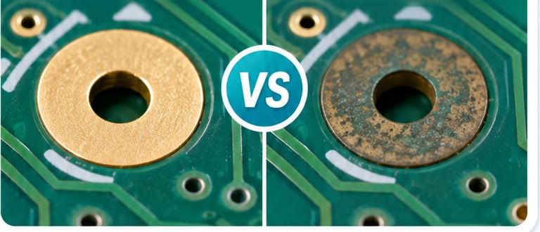
Hates storage. Once unpacked, assemble within ~24 hours; total shelf life is typically only 3–6 months
Hates multiple reflows. The film degrades with each thermal cycle — 2–3 passes is usually the limit; plan your sequence carefully on double-sided boards with wave soldering
Hates fingerprints and humidity. Sweat and handling destroy the film — pads discolor and "change face"
The film is transparent, so incoming inspection can't judge it visually
Repeated test-probe contact punctures the film and exposes copper
No wire bonding, no contact/keypad surfaces
Best fit
High-volume, fast-turn consumer electronics (smartphone mainboards use OSP heavily)
Projects with stable line takt and tightly controlled storage windows
Avoid for prototypes, R&D boards, and small batches — let a board sit too long and the pads are gone
3. ENIG — Electroless Nickel Immersion Gold
Strengths
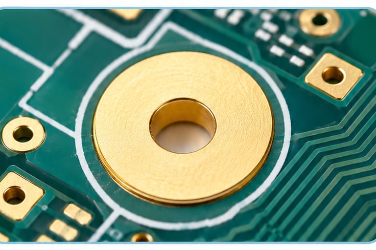
Excellent planarity — a first choice for fine-pitch and BGA
Long shelf life (12 months), tolerates multiple reflows, wide process window
The nickel layer serves as a barrier and wear surface — usable for keypads and contacts
Supports aluminum wire bonding; clean appearance, easy to inspect
Traps
Noticeably more expensive than HASL and OSP
Black pad. Phosphorus segregation plus hyper-corrosion in the nickel layer causes brittle joint fracture — often surfacing only after assembly, or worse, in the field. Qualify your fab: mid-phosphorus nickel (7–9% P) and controlled gold thickness are non-negotiable
Nickel corrosion. Risk rises under high voltage, high current, and harsh environments
The joint interface is tin-nickel IMC — more brittle than tin-copper. Evaluate carefully for high mechanical stress or frequent mating
Nickel is magnetic and lossy at high frequency — skin-effect losses matter on RF/mmWave boards
More gold is not better: excess gold embrittles joints. Keep it around 0.05–0.1 µm
Best fit
Fine-pitch BGA, QFN, high-density HDI boards
Long storage requirements; high-mix, low-volume production
Keypad boards, contact surfaces, aluminum wire bonding
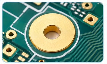
4. Immersion Silver (ImAg)
Strengths
Flat, highly solderable; silver dissolves into the joint, leaving a strong tin-copper IMC
Outstanding high-frequency performance — no nickel layer means low signal loss; a favorite for RF boards
Cost sits between OSP and ENIG
Traps
Hates sulfur and contamination. Sulfur in the environment (rubber, cardboard, industrial air) tarnishes silver and drives galvanic corrosion
Strict storage: vacuum packaging with anti-tarnish paper; solder within 24–48 hours of unpacking
Silver migration. Under humidity plus electrical bias, silver ions migrate and can short fine traces — evaluate for high-voltage, fine-line designs
Micro-voiding (champagne voids) appears under certain process conditions
Gloves are mandatory — a fingerprint scraps the board
Best fit
RF / high-frequency boards, where the no-nickel advantage is decisive
Fine-pitch, cost-sensitive projects with controlled handling and storage
5. Immersion Tin (ImSn)
Strengths
Flat and solderable, with a direct tin-copper interface
The best finish for press-fit connectors — the ductile tin layer suits compliant-pin holes
Moderate cost; common in automotive and backplane products
Traps
Tin-copper diffusion. Tin keeps converting to IMC in storage, thinning the solderable layer — shelf life is roughly 6 months, and after the first reflow, complete remaining soldering steps promptly
Tin whisker risk: pure tin under stress grows whiskers that can micro-short
The chemistry contains thiourea — demands solid wastewater handling and process control at the fab
Limited reflow capability (≤ 2 cycles is the safe assumption)
Watch compatibility with solder mask and potential attack on mask dams
Best fit
Backplanes and automotive electronics with heavy press-fit connector use
Projects needing high planarity on a budget below ENIG
6. Advanced Options: ENEPIG / Hard Gold / Soft Gold
ENEPIG (Electroless Nickel Electroless Palladium Immersion Gold). A palladium layer between nickel and gold essentially eliminates black pad and supports gold wire bonding — often called the "universal finish." The price of universality is cost. First choice for mixed soldering-plus-bonding boards.
Electrolytic hard gold. Purpose-built for edge connectors ("gold fingers") and plug interfaces — survives up to thousands of mating cycles. Selective only (requires plating bars), and expensive.
Electrolytic soft gold. For gold wire bonding and COB — thick, high-purity gold at the highest cost.
Real projects often use combination finishes: ENIG plus hard-gold fingers, or OSP with selective ENIG — different treatments for different functional zones.
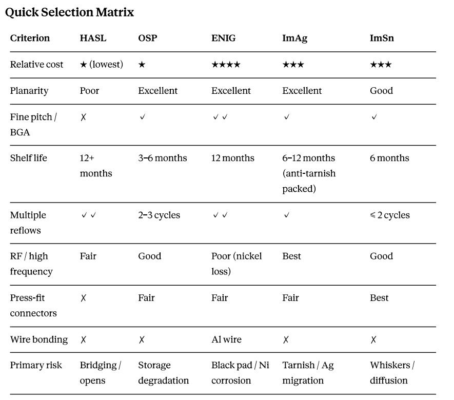
Conclusions by Scenario (Decision-Makers, Start Here)
High-volume consumer electronics, pitch ≥ 0.65 mm, cost first → Lead-free HASL
High volume, fine pitch, fast line turnover, controlled storage → OSP
Prototypes, R&D boards, small batches, uncertain assembly dates → ENIG (not OSP — pads degrade on the shelf)
Fine-pitch BGA / HDI / high-mix low-volume → ENIG, with fab qualification on nickel-phosphorus control
RF / high frequency / mmWave → Immersion silver first; assess nickel loss before choosing ENIG
Backplanes / automotive / heavy press-fit use → Immersion tin
Mixed soldering + gold wire bonding → ENEPIG
Gold fingers, frequent mating interfaces → Selective hard gold on the connector zone, another finish for the body
High voltage, high current, repeated mating, harsh environments → Be cautious with plain ENIG; assess nickel corrosion, consider combination finishes or heavier deposits
Five Questions to Ask Before You Place the Order
What's the smallest pitch on the board? Any BGA/QFN? — Determines whether HASL is even on the table
How long will boards sit between fabrication and assembly? Any second-pass assembly or rework? — Rules OSP and immersion tin in or out
How many reflow cycles? Any wave or selective soldering? — Check against each finish's process window
Any high-frequency signals, press-fit holes, gold fingers, or wire bonding? — These are hard exclusion criteria
What's the end-use environment? (Humidity, sulfur exposure, high voltage, vibration, mating frequency) — Determines long-term reliability
The Bottom Line
There is no universal surface finish — only a finish that matches your design, your process, and your product's life in the field.
Choose wrong, and the factory can only "build to print." When problems surface later, the conversation too often shrinks to a single sentence: "Why is this board so hard to solder?"
Treat surface finish as a design decision, not a line item on a purchase order. That decision is half of whether your board survives mass production.
SERVICES
Peakingtech © 2025. · Shenzhen, China · Privacy Policy · Terms of Service
Contact Form
Metal Parts


Peakingtech® is a registered trademark of Peakingtech Co in the United States.
COMPANY
CONTACT