
How to Select ESD Protection for USB Ports: A Practical Guide for Hardware Engineers
USB ESD protection isn't mysterious. The core idea is simple: intercept the transient before it reaches your main chip, shunt the current to ground as fast as possible, and do it without degrading your high-speed signals.
PRODUCT DEVELOPMENT
Peakingtech Engineering Team
7/10/20264 min read
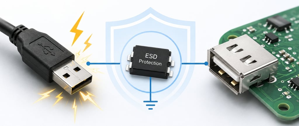
USB ports take more abuse than almost any other interface on a product. They're constantly touched by cables, chargers, laptops, docks — and human fingers. Every one of those contacts is a potential electrostatic discharge event, and once a strike enters through the connector, it can travel down D+, D−, the SuperSpeed differential pairs, CC, SBU, or VBUS straight into your downstream ICs. The symptoms range from annoying (communication glitches, failed enumeration) to serious (lockups, resets, permanently damaged interface chips).
The good news is that USB ESD protection isn't mysterious. The core idea is simple: intercept the transient before it reaches your main chip, shunt the current to ground as fast as possible, and do it without degrading your high-speed signals. The tricky part is that "USB" isn't one thing — different USB generations, different lines within the same connector, and different operating voltages all call for different selection priorities. Treat them all the same and you'll either fail ESD testing or fail signal integrity. This guide walks through how to get both right.
Not All USB Lines Are Created Equal
Before picking any part, map out what you're actually protecting. A USB Type-C connector alone carries at least five distinct categories of lines, each with its own risk profile:
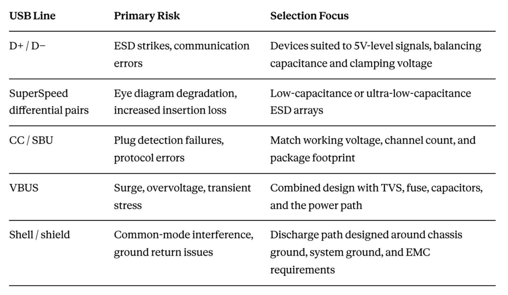
The single most common mistake is picking one ESD diode and sprinkling it across every line. VBUS, CC, SBU, and high-speed data lines differ in voltage, speed, and capacitance tolerance — they need to be selected line by line.
The Four Parameters That Actually Matter
Datasheets for ESD protection devices are dense, but for USB applications the decision comes down to four numbers.
Reverse working voltage (VRWM). The device's VRWM must sit above the normal operating voltage of the line it protects, otherwise it will leak during normal operation. For D+, D−, and high-speed data lines, size VRWM to the signal level. VBUS is a different animal: evaluate it separately against 5V, your fast-charging voltage, or whatever the system's maximum working voltage is. A part that's fine on a data line can be completely wrong on a Power Delivery VBUS rail.
Junction capacitance (Cj). This is where USB generation matters most. USB 2.0 data lines are relatively forgiving; USB 3.0 and faster interfaces are not. On SuperSpeed pairs, excess junction capacitance shows up directly as insertion loss, impedance discontinuity, and a closing eye diagram. For those lines, low-capacitance or ultra-low-capacitance ESD devices should be your default, not an upgrade.
Clamping voltage (VC). The clamping voltage needs to stay below the transient voltage your downstream chip can survive. One caveat that catches people: the clamping voltage on the datasheet isn't the whole story. Real-world clamping performance also depends on the ESD device's path to ground — trace length, trace width, and via count all add parasitic inductance that lets the voltage spike higher than the datasheet suggests.
Package and channel count. Space around a USB connector is always tight, which is why small DFN and SOD packages and multi-channel ESD arrays dominate this application. Multi-channel arrays work well when differential lines cluster together and can be protected as a group; discrete small-package parts make more sense when lines are physically scattered or you're protecting a single trace.
Selection Guidelines by Application
Here's how those priorities translate into concrete recommendations across common USB scenarios:
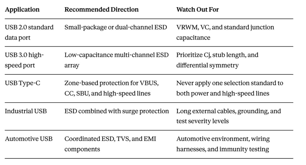
Notice the pattern: as the environment gets harsher (industrial, automotive), ESD protection stops being a standalone component choice and becomes part of a coordinated protection scheme involving TVS diodes, surge handling, and EMI suppression.
Layout Makes or Breaks the Design
You can select the perfect device and still fail ESD testing with poor placement. A few principles are non-negotiable.
Place the ESD device as close to the connector as physically possible. The goal is to bleed off the strike before the current ever enters the board's inner routing. Every millimeter between the connector and the protection device is a millimeter of your board the transient gets to travel unimpeded — and the further the device sits from the connector, the more likely the discharge reaches your traces and downstream silicon first.
Keep the path to ground short, wide, and direct. Long, thin traces between the ESD device and ground add parasitic inductance, and inductance is exactly what lets the clamped voltage overshoot during the fast edge of an ESD event.
On USB 3.0 and faster differential pairs, keep the stub connecting the ESD device as short as possible, maintain symmetry between the two lines of each pair, and avoid long branches and unnecessary vias. Asymmetry and stubs show up as mode conversion and reflections at these speeds.
For VBUS, don't place the protection device in isolation. Lay it out as part of the complete power path — together with bulk capacitance, the fuse, and the downstream power IC — so surge energy is handled at the entry point rather than slamming into the system's interior.
Common Questions
Can I use the same ESD diode on every line of a USB port?
Not recommended. VBUS, CC, SBU, D+, D−, and the high-speed differential pairs differ in voltage, data rate, and capacitance tolerance. Select per line, or per group of electrically similar lines.
Why do USB 3.0 ports specifically need low-capacitance ESD devices?
SuperSpeed differential pairs are sensitive to signal integrity. Excess junction capacitance increases insertion loss and degrades the eye diagram — which means link errors, failed compliance testing, or reduced margin in the field.
Is it okay to place the ESD device a bit further from the connector?
Not recommended. The greater the distance, the more likely the static discharge enters the board's routing and reaches downstream chips before it can be shunted, and protection effectiveness drops accordingly.
The Bottom Line
ESD selection for USB comes down to a discipline of matching: match VRWM to the line's working voltage, match capacitance to the line's data rate, match clamping voltage to what the downstream chip can survive, and match the layout to the physics of a nanosecond-scale transient. Do the line-by-line homework up front, and ESD compliance testing becomes a formality instead of a fire drill.
SERVICES
Peakingtech © 2025. · Shenzhen, China · Privacy Policy · Terms of Service
Contact Form
Metal Parts


Peakingtech® is a registered trademark of Peakingtech Co in the United States.
COMPANY
CONTACT