
Copper Coin PCBs: When Thermal Vias Aren't Enough for Power Electronics
If you design boards that carry serious power, you've probably met this problem: a power device running too hot to touch, an FR4 substrate that refuses to move heat, and a thermal via array that helps — but not enough.
ELECTRONICS MANUFACTURING
Peakingtech Engineering Team
7/10/20265 min read
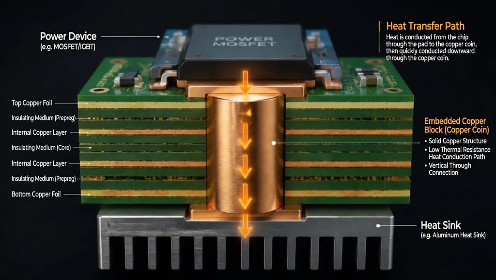
If you design boards that carry serious power, you've probably met this problem: a power device running too hot to touch, an FR4 substrate that refuses to move heat, and a thermal via array that helps — but not enough.
The usual escalation path is familiar. Thicken the copper to 4 oz or 6 oz. Pack thermal vias under the pad until the footprint looks like a honeycomb. Bolt on an external heatsink. All of these work to a point, and all of them hit a ceiling. Above 6 oz copper, etching precision and lamination difficulty climb sharply. Thermal vias are limited by their plated barrel walls — typically just 25–35 μm of copper — which caps their effective thermal conductivity at roughly 20–40 W/mK. Compare that to solid copper at 401 W/mK and you're an order of magnitude short.
That gap is why a more direct approach keeps showing up on high-power boards: the embedded copper coin.
Where the Heat Path Breaks Down
To appreciate the copper coin solution, it helps to see how bad the baseline is.
FR4 has a thermal conductivity of roughly 0.3–0.4 W/mK. Copper sits at 401 W/mK — about a thousand times higher. For the same cross-section, copper moves a thousand times more heat per second than the laminate around it.
On a standard PCB, heat from a power device travels through a chain: device junction → solder layer → copper pad → thermal vias or copper foil → FR4 dielectric → bottom copper → heatsink. Every FR4 layer in that chain adds a large chunk of thermal resistance. Once device power exceeds about 10 W, the temperature deltas along this path stack up quickly to unacceptable levels.
The instinctive fix — more thermal vias — runs into a geometry problem. A via conducts heat only through its thin plated wall. It's like trying to move a large volume of water through a pipe whose wall is only 0.3 mm thick: the bottleneck isn't the pipe's diameter, it's how little material is actually doing the work.
The Copper Coin: A Thermal Highway Through the Board
The copper coin approach (also called copper inlay or embedded copper block) is conceptually simple: embed a solid block of copper directly beneath the heat-generating device, running from the device pad straight through to the board bottom or heatsink.
That block conducts at 401 W/mK. Against FR4's 0.3 W/mK, it's the difference between a dirt road and an eight-lane expressway.
There are three main structural implementations:
Embedded coin. A precision cavity is milled into the inner layers, and the coin is inset so its top face sits flush with the device pad while its bottom face contacts an inner copper layer or the bottom copper. This suits single-sided heat extraction and demands manufacturing tolerances around ±0.05 mm.
Through-type coin. The coin spans the full board thickness, top to bottom, with no internal interfaces. This delivers the lowest thermal resistance of the three and fits the classic arrangement of device on top, heatsink on the bottom.
Multi-coin arrays. When a power module contains several heat sources — the multiple dies of an IGBT module, for example — a coin is placed directly under each one, creating parallel thermal channels. Adequate spacing between coins prevents thermal coupling.
What the Numbers Say
Measured results are more persuasive than theory. Test data published by multiple PCB fabricators and power module suppliers converge on the following:
Board-level thermal resistance drops from a conventional 0.8–1.2 K/W to 0.3–0.5 K/W — a reduction of 40–60%. For power devices in the 200 W class, copper coin designs cut junction temperature by 15–30 °C. Compared with an equivalent thickness of FR4, thermal transfer capability improves 10–20×. And against a well-designed thermal via array, the coin's junction-to-case thermal resistance comes in 30–50% lower.
One data point from the extreme end: OKI Circuit Technology in Japan published 2024 test results for a stepped copper coin structure that achieved 55× the heat dissipation of a conventional PCB in vacuum — developed specifically for spaceborne electronics where convection cooling is impossible.
Sizing is straightforward in practice. Coin diameter typically matches the device footprint, usually 5–25 mm. Thickness runs 1.0–3.0 mm depending on board stack-up and power level: a 1.5 mm coin handles most 20–50 W dissipation scenarios, and only extreme power densities above 100 W/cm² call for 2.5–3.0 mm.
Not Every Board Needs One
Copper coins have a clear applicability boundary, and they add a precision milling and inlay step to fabrication, so they should be specified deliberately.
They earn their cost when power density exceeds roughly 10 W per device (SiC MOSFETs, IGBTs, GaN power transistors), when Z-axis space rules out a heatsink or fan, when multiple heat sources are concentrated in one module (power modules, DC-DC converters), or when the enclosure is sealed and convection isn't available — outdoor equipment and hermetic packages being the common cases.
They're usually not worth it below about 5 W per device, where thermal vias are perfectly adequate; on high-volume, cost-driven products where the added inlay process hurts unit economics; or on non-standard board thicknesses that would require custom coin geometries.
From Coins to Busbars: Point Solutions vs. Line Solutions
At this point a reasonable question comes up: the coin is embedded inside the board — could you instead put copper on top of it?
You can. That's the coin's close relative: the SMD copper busbar.
Where the coin takes the embedded route — opening a channel inside the board — the busbar takes the surface-mount route, placed on the board like any other SMT component and soldered in reflow. Both exploit the same two properties of copper: high thermal conductivity to move heat, low electrical resistance to carry current.
The difference is the shape of the problem they solve. A copper coin is a point solution — it relieves the local thermal bottleneck directly beneath a single hot device. An SMD busbar is a line solution — it carries high current along a route, handles parallel current sharing across multiple paths, and provides low-impedance connections in power loops.
A concrete example: if your board needs to route a 100 A bus and no practical trace width can carry it, a copper coin won't help — that's busbar territory. If a single IGBT is running hot and the via array under it has maxed out, that's coin territory. One handles points, the other handles lines, and they don't conflict.
Typical SMD busbar applications include inverters, DC-DC converters, and battery management systems — anywhere multiple parallel bars carry bus-level current across the board. Commercially available parts span roughly 3 A signal-level up to 200 A power-level ratings, in lengths from a few millimeters to 30 mm and beyond, usually nickel-plated brass or nickel-plated pure copper supplied in tape-and-reel for standard SMT placement.
The Takeaway
High current and high power on a PCB make thermal management unavoidable. The copper coin attacks the problem in the most direct way possible — putting a solid piece of copper right where the heat is generated and giving it a straight path out of the board. It isn't complicated, but it works.
And when the bottleneck isn't a hot point but a current-carrying line, SMD copper busbars fill that role. Used together, the two cover most of the thermal and current-carrying corner cases on high-power boards.
If you're moving a power design into production and weighing copper coin fabrication, heavy copper, or busbar assembly options, this is exactly the kind of DFM trade-off worth settling before the first prototype run.
SERVICES
Peakingtech © 2025. · Shenzhen, China · Privacy Policy · Terms of Service
Contact Form
Metal Parts


Peakingtech® is a registered trademark of Peakingtech Co in the United States.
COMPANY
CONTACT