Ultimate Guide to OSP for PCB Design and Manufacturing
Among the various surface finish options, Organic Solderability Preservative (OSP) stands out for its cost-effectiveness, eco-friendliness, and compatibility with modern soldering processes.
ELECTRONICS MANUFACTURING
4/11/20258 min read
In the fast-paced world of electronics manufacturing, ensuring reliable and cost-effective printed circuit board (PCB) assembly is paramount. One critical aspect of PCB fabrication is the surface finish, which protects copper surfaces from oxidation while maintaining solderability during assembly. Among the various surface finish options, Organic Solderability Preservative (OSP) stands out for its cost-effectiveness, eco-friendliness, and compatibility with modern soldering processes. This guide dives deep into OSP, offering designers, engineers, and decision-makers a detailed application roadmap to leverage OSP effectively in electronics development projects.
What is OSP and Why Does It Matter?
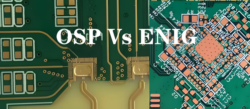
OSP is a surface treatment process that applies a thin organic coating to exposed copper surfaces on a PCB. This protective layer, typically 0.2–0.5 micrometers thick, prevents oxidation while ensuring the copper remains solderable during assembly. Unlike metallic finishes like Hot Air Solder Leveling (HASL), Electroless Nickel Immersion Gold (ENIG) or immersion silver, OSP uses organic compounds, such as benzotriazole or imidazole derivatives, to form a chemical barrier.
OSP has gained traction in industries ranging from consumer electronics to automotive and IoT devices due to its unique blend of advantages, including low cost, environmental friendliness, and excellent solderability. However, its limitations—such as limited thermal stability and shelf life—require careful consideration during design, manufacturing, and assembly. This guide will walk you through the OSP process, its pros and cons, key application guidelines, and emerging trends to help you make informed decisions.
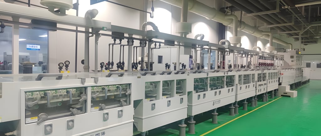
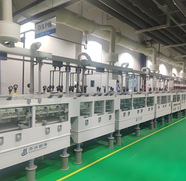
Understanding the OSP Process Flow
To appreciate OSP’s role in PCB manufacturing, let’s break down the process flow, which consists of four primary steps:
1. Copper Surface Cleaning
The process begins with cleaning the copper surfaces to remove oxides, oils, and other contaminants. Acidic or alkaline cleaning agents are typically used to ensure a pristine surface. A clean copper surface is critical, as any residual contaminants can compromise the adhesion and uniformity of the OSP coating.
Key Consideration: Ensure the cleaning process is optimized to avoid over-etching, which can damage the copper or alter pad dimensions.
2. Microetching
Next, the copper surface undergoes microetching to enhance roughness, improving the adhesion of the OSP film. Microetching solutions, such as sulfuric acid-hydrogen peroxide or sodium persulfate-based chemistries, create a slightly textured surface without significantly altering the copper’s thickness.
Key Consideration: Control the microetching rate to achieve consistent surface roughness without compromising trace integrity, especially for fine-pitch designs.
3. OSP Coating
The PCB is immersed in an OSP solution containing organic acids (e.g., benzotriazole or imidazole derivatives). These compounds chemically bond with the copper, forming a protective film approximately 0.2–0.5 μm thick. The coating process is typically performed in a controlled bath to ensure uniformity across all exposed copper surfaces.
Key Consideration: Monitor bath chemistry and immersion time to maintain the desired film thickness, as deviations can affect solderability or oxidation resistance.
4. Drying and Inspection
After coating, the PCB is dried to stabilize the OSP film. Inspection follows to verify film thickness, uniformity, and thermal resistance. Techniques like UV spectroscopy or electrochemical methods are used to assess coating quality, ensuring compliance with soldering requirements.
Key Consideration: Implement robust inspection protocols, as the transparent nature of OSP makes visual assessment challenging.
Advantages of OSP: Why Choose It?
OSP offers several compelling benefits that make it a preferred choice for many electronics projects. Here’s a closer look at its advantages:
1. Cost-Effectiveness
Compared to metallic finishes like ENIG or immersion silver, OSP requires fewer chemicals and simpler equipment, reducing production costs. This makes it an attractive option for high-volume manufacturing, particularly for consumer electronics.
For Decision-Makers: OSP’s lower cost can improve profit margins or allow reinvestment in other project areas, such as advanced components or design enhancements.
2. Eco-Friendliness
OSP is a water-based process that generates low-toxicity waste, aligning with environmental regulations and sustainability goals. Unlike processes involving heavy metals (e.g., nickel or gold), OSP minimizes hazardous byproducts, reducing disposal costs and environmental impact.
For Engineers: Choosing OSP can streamline compliance with RoHS and other environmental standards, simplifying certification processes.
3. Superior Solderability
During soldering, the OSP film dissolves rapidly in flux, exposing fresh copper for excellent solder wetting. This ensures strong, reliable solder joints, critical for high-yield assembly.
For Designers: OSP’s solderability supports a wide range of assembly techniques, including surface-mount technology (SMT) and through-hole soldering, without requiring specialized fluxes.
4. Rework Compatibility
OSP-coated PCBs can undergo multiple rework cycles, as fresh solder can still wet the copper pads even after initial soldering. This flexibility is valuable for prototypes or products requiring post-assembly modifications.
For Engineers: OSP’s rework compatibility reduces scrap rates during development, saving time and resources.
Limitations of OSP: What to Watch Out For
While OSP offers significant advantages, it’s not without challenges. Understanding its limitations is crucial for successful implementation:
1. Poor Thermal Stability
The OSP film degrades under high temperatures or multiple reflow cycles, which can compromise solderability. This is particularly problematic for double-sided SMT assembly or lead-free soldering, which requires higher peak temperatures.
Mitigation Strategy: Optimize reflow profiles to keep peak temperatures below 245°C and minimize dwell time to preserve the OSP film.
2. Short Shelf Life
OSP-coated PCBs have a limited shelf life, typically 3–6 months, as prolonged exposure to air can cause copper oxidation beneath the film. This constraint requires tight inventory management and rapid assembly timelines.
Mitigation Strategy: Use moisture-proof packaging and store PCBs in controlled environments (low temperature and humidity) to extend shelf life.
3. Inspection Challenges
The transparent OSP film is difficult to inspect visually, necessitating specialized tools like thickness measurement devices or spectroscopic equipment. Inconsistent film thickness can lead to soldering defects or premature oxidation.
Mitigation Strategy: Invest in automated inspection systems to ensure coating uniformity, particularly for high-reliability applications.
4. Electrical Testing Issues
The insulating OSP film can impede test probe contact during in-circuit testing (ICT), leading to false failures. This requires additional design considerations, such as solder mask openings or local solder paste application at test points.
Mitigation Strategy: Collaborate with test engineers to incorporate test-friendly features during PCB layout, minimizing testing bottlenecks.
Key Application Guidelines for OSP Success
To maximize OSP’s benefits while mitigating its limitations, designers, engineers, and decision-makers should follow these application guidelines:
1. Process Control
Maintaining the OSP film thickness within the optimal range of 0.2–0.5 μm is critical. Excessive thickness can hinder solderability by preventing the film from dissolving completely during soldering, while insufficient thickness reduces oxidation resistance.
For Engineers: Work closely with PCB fabricators to monitor bath chemistry, immersion time, and drying conditions. Implement statistical process control (SPC) to track coating consistency.
For Decision-Makers: Invest in quality assurance tools, such as film thickness analyzers, to ensure process reliability without significantly increasing costs.
2. Soldering Optimization
OSP performs best when soldering conditions are carefully controlled. Lead-free soldering, which typically requires temperatures above 240°C, can stress the OSP film, leading to incomplete dissolution or copper exposure.
For Designers: Specify reflow profiles with peak temperatures ≤245°C and short dwell times to preserve the OSP film. Consider nitrogen reflow atmospheres to reduce oxidation risks.
For Engineers: Validate soldering parameters during pilot runs, using thermal profiling tools to ensure consistent results across production batches.
3. PCB Design Adjustments
OSP’s unique properties require specific design considerations to ensure manufacturability and testability:
Pad Size and Spacing: Optimize pad dimensions and spacing to minimize thermal stress during soldering, particularly for dense, fine-pitch layouts.
Test Point Accessibility: Reserve solder mask openings or apply local solder paste at test points to ensure reliable probe contact during ICT.
Component Placement: Avoid placing high-power components near OSP-coated pads, as localized heating can degrade the film.
For Designers: Use design-for-manufacturing (DFM) tools to simulate thermal and electrical performance, ensuring OSP compatibility with your layout.
For Engineers: Collaborate with design teams to review Gerber files for OSP-specific adjustments before fabrication.
4. Storage and Packaging
Proper storage and handling are essential to maintain OSP-coated PCBs’ integrity before assembly.
Storage Conditions: Store PCBs in moisture-proof packaging at temperatures below 30°C and relative humidity below 60%. Avoid prolonged exposure to air, especially in humid climates.
Assembly Timeline: Complete assembly within 24 hours of opening the package to minimize oxidation risks.
For Decision-Makers: Partner with logistics providers to ensure proper storage during transit, particularly for global supply chains.
For Engineers: Implement first-in-first-out (FIFO) inventory practices to prioritize older PCBs, reducing waste due to expired shelf life.
OSP in Action: Real-World Applications
OSP is widely used across various industries, each leveraging its strengths to meet specific needs:
Consumer Electronics: Smartphones, tablets, and wearables benefit from OSP’s low cost and compatibility with high-volume SMT assembly.
Automotive Electronics: OSP supports robust solder joints for sensors and control modules, though careful process control is needed for lead-free soldering.
IoT Devices: OSP’s eco-friendliness aligns with the sustainability goals of connected devices, while its rework compatibility aids prototyping.
Industrial Equipment: OSP-coated PCBs in control systems benefit from reliable solderability, though extended shelf life may require enhanced formulations.
Case Study Example: A leading smartphone manufacturer adopted OSP for its mid-range product line, reducing fabrication costs by 15% compared to ENIG while maintaining a 99.8% assembly yield. By optimizing reflow profiles and implementing nitrogen atmospheres, the company mitigated thermal stability concerns, ensuring reliable performance.

Future Developments in OSP Technology
As electronics evolve toward higher reliability, miniaturization, and sustainability, OSP technology is advancing to meet these demands. Here are some exciting trends to watch:
1. Enhanced Thermal Resistance
Researchers are developing OSP formulations that withstand temperatures above 300°C, enabling compatibility with advanced packaging techniques like system-in-package (SiP) and chip-on-board (CoB). These high-temperature coatings will expand OSP’s use in automotive and aerospace applications.
For Decision-Makers: Monitor these developments to future-proof your supply chain, as thermally robust OSP could reduce reliance on costlier finishes.
2. Extended Shelf Life
New OSP solutions incorporate antioxidant additives or composite coatings to improve film stability, extending shelf life beyond 12 months. This will simplify inventory management and reduce waste, particularly for low-volume or seasonal products.
For Engineers: Evaluate extended-shelf-life OSP options during supplier qualification to balance cost and performance.
3. Smart Inspection
Emerging optical and electrochemical inspection methods enable real-time monitoring of OSP film thickness and uniformity. These smart systems integrate with Industry 4.0 frameworks, providing data-driven insights to optimize fabrication.
For Designers: Leverage inspection data to refine DFM guidelines, ensuring consistent OSP performance across complex layouts.
Making the Right Choice: Is OSP for Your Project?
Deciding whether OSP is the right surface finish for your project requires weighing its benefits against its constraints. Here’s a quick checklist to guide your decision:
Choose OSP If:
Cost reduction is a priority, especially for high-volume production.
Your project aligns with eco-friendly manufacturing goals.
Your assembly process supports single-sided or low-reflow-cycle soldering.
Rework flexibility is valuable, such as during prototyping.
Consider Alternatives If:
Your PCBs require a shelf life exceeding 6 months.
Your design involves multiple high-temperature reflow cycles.
In-circuit testing is critical, and test point modifications are impractical.
Your application demands ultra-high reliability (e.g., aerospace or medical).
Pro Tip: Collaborate with your PCB fabricator and assembly partner early in the design phase to validate OSP compatibility with your specific requirements.
Conclusion: Empowering Your Electronics Journey with OSP
OSP is a versatile, cost-effective, and environmentally friendly surface finish that empowers electronics designers, engineers, and decision-makers to deliver high-quality PCBs. By understanding its process flow, leveraging its advantages, and addressing its limitations through thoughtful design and process control, you can unlock OSP’s full potential in your projects. As OSP technology continues to evolve—offering improved thermal resistance, extended shelf life, and smarter inspection—its role in modern electronics manufacturing will only grow.
Whether you’re developing the next generation of consumer gadgets, automotive systems, or IoT solutions, OSP offers a compelling balance of performance and practicality. Armed with this guide, you’re well-equipped to integrate OSP into your workflow, ensuring reliable, sustainable, and cost-efficient outcomes for your electronics development journey.
SERVICES
Peakingtech © 2025. · Shenzhen, China · Privacy Policy · Terms of Service
Contact Form
Metal Parts
Peakingtech® is a registered trademark of Peakingtech Co in the United States.
COMPANY
CONTACT