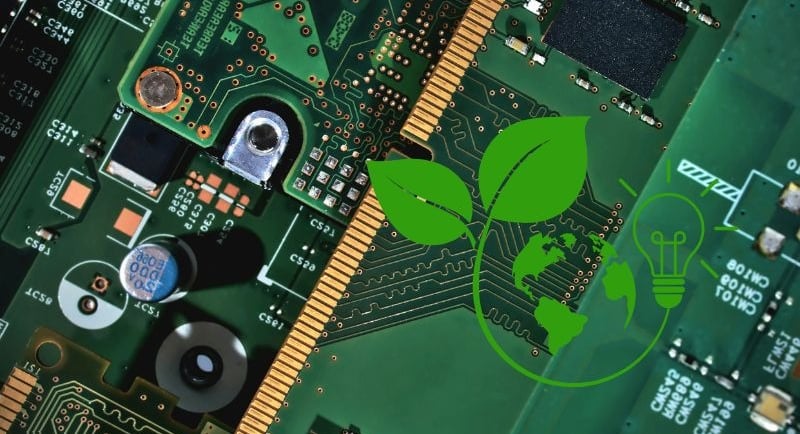
The Future of Green Electronics: Revolutionizing PCB Manufacturing for Sustainability
As the backbone of modern electronics, PCBs are essential components found in virtually every electronic device. However, their traditional manufacturing processes often involve toxic materials and generate significant waste, posing serious risks to both human health and the environment.
2/1/20253 min read
In today's increasingly eco-conscious world, the electronics industry faces a critical challenge: making printed circuit board (PCB) manufacturing more sustainable. As the backbone of modern electronics, PCBs are essential components found in virtually every electronic device. However, their traditional manufacturing processes often involve toxic materials and generate significant waste, posing serious risks to both human health and the environment.
The Environmental Impact of PCB Manufacturing
The environmental footprint of PCB production is substantial and multifaceted. Traditional manufacturing processes rely heavily on hazardous materials, including:
Lead in soldering
Brominated flame retardants (BFRs)
Toxic solvents and chemicals
Heavy metals that can leach into soil and water systems
These materials pose immediate risks during manufacturing through worker exposure and chemical releases. Moreover, they create long-term challenges in electronic waste management, as improper disposal can lead to environmental contamination. Studies have shown that a single PCB can contaminate up to 50 square meters of soil and 65,000 liters of groundwater if not properly handled. The electronic waste crisis is particularly severe in developing countries, where informal recycling practices often expose workers and communities to dangerous toxins.
Current Industry Approaches and Their Limitations
While the industry has made some progress toward sustainability, many current initiatives focus primarily on regulatory compliance rather than comprehensive environmental responsibility. Several common approaches include:
Lead-Free Soldering
The adoption of lead-free solders, particularly SAC (tin-silver-copper) alloys, has become widespread due to regulations like RoHS. However, this solution introduces new challenges, as the mining and extraction of alternative materials can cause significant environmental damage and may result in less reliable solder joints.
Recycling Programs
Though electronics recycling programs help recover valuable materials, recent data from the Global E-waste Monitor 2024 shows a concerning trend: the documented collection and recycling rate is expected to decline from 22.3% in 2022 to 20% by 2030. This highlights the need for more comprehensive solutions beyond end-of-life management.
Material Alternatives
The industry has explored options like halogen-free laminates to reduce toxicity. However, these alternatives often come with their own drawbacks, including reduced performance and potential increases in non-recyclable waste.
Innovative Solutions for a Sustainable Future
To truly address these challenges, the industry needs to move beyond simple compliance and embrace more innovative, holistic approaches to sustainability:
Bio-Based Materials
One of the most promising developments is the emergence of bio-based PCB materials. These include:
Substrates made from cellulose and lignin, which can reduce carbon footprint by up to 35%
Natural polymer-based components derived from renewable resources like corn starch and vegetable oils
Bio-based resins with properties comparable to traditional epoxy, offering thermal stability up to 180°C
These materials offer significant environmental benefits while maintaining necessary performance characteristics. Research shows that bio-based PCB materials can decompose up to 80% within six months under proper conditions, compared to hundreds of years for traditional materials. Furthermore, their production typically requires 40-60% less energy than conventional materials.
Green Chemistry Integration
The application of green chemistry principles is revolutionizing PCB manufacturing through:
Water-based solutions replacing toxic solvents, reducing volatile organic compound emissions by up to 70%
Supercritical fluid applications that eliminate the need for harsh chemical cleaners
Additive manufacturing techniques that minimize waste, reducing material consumption by up to 40%
Advanced 3D printing processes enabling complex, material-efficient designs that optimize performance while reducing environmental impact
Circular Manufacturing
A circular approach to PCB manufacturing focuses on:
Designing for disassembly and material recovery, enabling up to 90% component reuse
Implementing modular components for easier upgrades, extending product lifespan by 2-3 times
Creating closed-loop material systems that can reduce raw material consumption by up to 60%
Developing local recycling partnerships to minimize transportation emissions and improve material recovery rates
Life Cycle Assessment (LCA)
Comprehensive LCA practices help manufacturers:
Evaluate environmental impacts at every stage, from raw material extraction to end-of-life disposal
Identify opportunities for improvement through detailed analysis of energy and material flows
Make data-driven sustainability decisions based on quantifiable environmental metrics
Optimize resource usage throughout the product lifecycle, potentially reducing overall environmental impact by 30-50%
Looking Ahead
The future of PCB manufacturing lies in balancing technical performance with environmental responsibility. While the transition to sustainable practices presents challenges, including initial investment costs and technical hurdles, it also offers opportunities for innovation and industry leadership. By embracing bio-based materials, green chemistry, circular manufacturing principles, and comprehensive lifecycle assessment, the electronics industry can work toward a future where technological advancement and environmental stewardship go hand in hand.
As we continue to rely more heavily on electronic devices, the importance of sustainable PCB manufacturing only grows. Industry leaders estimate that implementing comprehensive sustainability measures could reduce the sector's environmental impact by up to 70% by 2030. The industry's commitment to developing and implementing eco-friendly solutions will play a crucial role in shaping a greener, more sustainable future for electronics manufacturing. This transition requires collaboration across the supply chain, investment in research and development, and a long-term perspective that values environmental protection alongside economic performance.
The path to sustainable PCB manufacturing is complex but necessary. As technologies advance and environmental pressures mount, the industry must continue to innovate and adapt. The success of these efforts will determine not only the future of electronics manufacturing but also our ability to build a more sustainable technological infrastructure for generations to come.
SERVICES
Peakingtech © 2025. · Shenzhen, China · Privacy Policy · Terms of Service
Contact Form
Metal Parts
Peakingtech® is a registered trademark of Peakingtech Co in the United States.
COMPANY
CONTACT