Step-by-Step Guide to PCB Assembly: From Design to Final Product
This guide will take you through each critical step, from initial design to final product integration, highlighting best practices and common challenges along the way.
2/10/20254 min read
Printed Circuit Boards (PCBs) are the backbone of modern electronics, found in everything from smartphones to industrial machinery. The PCB assembly process is a complex but essential aspect of bringing electronic designs to life. Whether you're an engineer, designer, or manufacturer, understanding the journey from PCB design to production ensures efficiency, cost-effectiveness, and high-quality results.
This guide will take you through each critical step, from initial design to final product integration, highlighting best practices and common challenges along the way.
1. PCB Design Phase
1.1 Schematic Design & Layout
The first step in the PCB assembly process is designing a schematic and layout using specialized software. Popular PCB design software includes:
Altium Designer – Industry-standard for professional PCB development.
KiCad – Open-source and widely used for personal and small business projects.
Eagle – A favorite among hobbyists and startups for its ease of use.
Best practices for designing PCBs include:
Optimizing component placement to minimize signal interference.
Keeping trace lengths as short as possible for better performance.
Ensuring proper power and ground plane distribution to reduce noise.
1.2 Design for Manufacturability (DFM)
Before proceeding to fabrication, DFM guidelines help ensure that the design can be manufactured efficiently and without errors. Important considerations include:
Proper trace width and spacing to avoid electrical shorts.
Thermal management to prevent overheating.
Avoiding unnecessarily complex layouts that could lead to higher manufacturing costs.
1.3 Gerber File Preparation
Once the design is finalized, Gerber files are generated. These files act as blueprints for PCB fabrication. Alongside them, manufacturers require:
Drill files to define hole placements.
Bill of Materials (BOM) listing all necessary components for assembly.
2. Prototyping & Validation
2.1 Rapid Prototyping Methods
Before full-scale production, prototyping helps test the design. Common methods include:
Breadboarding – Useful for testing basic circuit functionality.
3D-printed prototypes – Helps in mechanical fitting before committing to mass production.
2.2 Design Iteration
Feedback from prototypes helps refine the final design. Engineers can tweak component placements, modify PCB traces, and ensure the board performs as intended before proceeding to full-scale fabrication.
3. Material Procurement
3.1 Component Sourcing
Selecting the right components involves balancing cost, quality, and lead times. Strategies to mitigate supply chain risks include:
Ordering from trusted suppliers with a track record of reliable delivery.
Considering alternative components in case of shortages.
Bulk purchasing to reduce costs.
3.2 PCB Substrate Selection
Different PCB materials are suited for different applications:
FR-4 – The most common substrate, offering good electrical insulation and mechanical strength.
High-frequency materials (e.g., Rogers) – Used for RF and microwave applications.
Aluminum or copper – Used for circuit board that generates a lot of heat, such as an LED light.
4. PCB Fabrication Process
4.1 Printing the Circuit Design
The PCB design is transferred onto copper-clad boards using photolithography, followed by etching to remove excess copper.
4.2 Multi-Layer PCB Lamination
For multi-layer PCBs, individual layers are aligned and bonded through a lamination process, ensuring precision and durability.
4.3 Drilling & Plating
Drilled holes (vias) are plated with conductive material to establish electrical connections between layers.
4.4 Solder Mask & Silkscreen Application
A solder mask is applied to protect copper traces, and a silkscreen layer is printed for component labeling and reference designators.
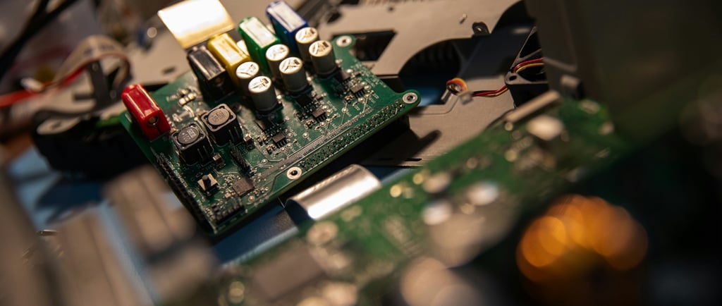
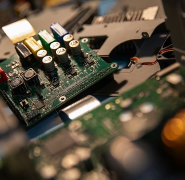
5. PCB Assembly Process
5.1 Solder Paste Application
A stencil printing process is used to apply solder paste precisely where surface mount components will be placed.
5.2 Component Placement
Modern pick-and-place machines ensure accurate placement of SMT components onto the PCB.
5.3 Reflow Soldering
The board passes through a reflow oven, where controlled heating melts the solder, securing components in place. Proper temperature profiling helps avoid defects like tombstoning (components lifting on one end).
5.4 Through-Hole Component Assembly
For components requiring strong mechanical bonds, wave soldering or manual soldering is used.
6. Testing & Quality Control
6.1 Automated Optical Inspection (AOI)
AOI systems scan the PCB to detect soldering defects, missing components, or misalignments.
6.2 In-Circuit Testing (ICT)
ICT involves probing test points on the board to validate electrical performance.
6.3 Functional Testing
Simulates real-world usage conditions to ensure the PCB meets all design requirements.
7. Final Product Integration
7.1 Enclosure Assembly
The PCB is mounted into the final product housing, ensuring all mechanical and electrical interfaces fit correctly.
7.2 Final Testing & Certification
Certifications such as FCC, CE, and UL confirm that the PCB meets industry safety and performance standards.
8. Common PCB Assembly Challenges & Solutions
Some common PCB assembly defects include:
Cold joints – Poor solder connections due to insufficient heat.
Solder bridges – Excess solder creating unintended connections.
Component tombstoning – Uneven heating causing components to lift.
Best practices for troubleshooting include visual inspections, thermal profiling, and adjusting reflow settings to improve soldering quality.
9. Future Trends in PCB Assembly
PCB manufacturing is evolving with advancements like:
AI-driven quality control – Reducing defects through machine learning algorithms.
Flexible PCBs – Enabling curved and wearable electronics.
Sustainable materials – Reducing environmental impact with biodegradable substrates.
Conclusion
The PCB assembly process requires precision at every step, from design to testing and final integration. Prioritizing DFM principles and collaborating with reliable manufacturers can help ensure a smooth, cost-effective, and high-quality production process.
Frequently Asked Questions
Q: How long does PCB assembly typically take?
A: The timeline varies significantly based on complexity and volume. A simple two-layer board might be assembled in a few days, while complex multilayer boards can take several weeks. With Peakingtech, we may complete prototyping of a typical simple PCBA within a week, thanks to our supply management and expertise in the industry.
Q: What's the main difference between SMT and through-hole assembly?
A: Surface-mount technology (SMT) places components directly onto the board's surface, while through-hole components have pins that go through holes in the board. SMT allows for higher component density and faster assembly.
Q: How do I choose between FR-4 and high-frequency PCB materials?
A: Consider your application's requirements. FR-4 is cost-effective and suitable for most applications, but high-frequency designs might require specialized materials like Rogers to maintain signal integrity.
SERVICES
Peakingtech © 2025. · Shenzhen, China · Privacy Policy · Terms of Service
Contact Form
Metal Parts
Peakingtech® is a registered trademark of Peakingtech Co in the United States.
COMPANY
CONTACT