Revolutionizing Sustainable Electronics with Laser-Patterned Wool Circuits
Discover how WoolTech, a biodegradable wool-based biomaterial developed by Hinna Khan, is transforming sustainable electronics. Learn how engineers can use laser-patterned wool to build flexible, eco-friendly circuits for wearables, sensors, and rapid prototyping.
IDEA TO DESIGN
8/6/20255 min read
1. Introduction: Wool Beyond Textiles
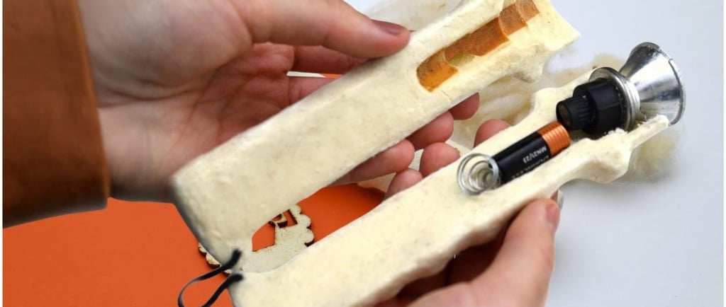
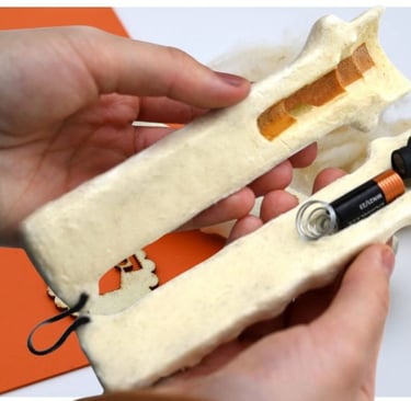
WoolTech, conceived by designer-engineer Hinna Khan, reimagines waste sheep wool as a biomaterial for building electronics without metal wiring, plastics, or traditional PCBs. Developed during Khan’s student design research, WoolTech offers a biodegradable and circular-material approach that addresses both resource waste and e‑waste environmental concerns.
While electronics engineers are accustomed to rigid, metal‑based conductive systems, WoolTech’s paradigm shift leverages a natural fiber system capable of hosting conductive paths—opening a new frontier in sustainable hardware design.
2. WoolTech: What It Is and How It Works
2.1 Core Concept
Waste Wool as Base: WoolTech uses surplus wool—otherwise discarded—to create casings, substrates, and insulation, replacing plastics and metals.
Laser‑Patterned Conductive Traces: Conductive pathways are directly patterned onto wool using laser activation of a conductive ink or coating, avoiding soldered metal wires.
Biodegradable Platform: Entire devices built with WoolTech can eventually biodegrade, leaving minimal ecological footprint.
2.2 Fabrication Steps
Raw Material Preparation: Clean and process waste wool fibers into sheets or molded forms.
Surface Treatment: Apply conductive precursor (e.g. carbon‑based ink, graphene dispersion).
Laser Scribing: Laser burns or cures the coating along designed circuit pathways, forming conductive tracks.
Assembly Integration: Mount discrete electronic components (e.g., LEDs, ICs) onto the wool substrate using extrusion‑friendly connectors or pressing techniques.
Sealing or Binding: Cover and protect the circuit with wool lid layers or natural adhesives.
This method eliminates plastic enclosures and metal connectors, relying instead on encapsulated components and traces embedded in the wool matrix.
3. Electrical & Material Properties
3.1 Conductivity and Performance
Although detailed electrical specs aren’t published yet, laser‑patterned carbon or graphene traces typically yield resistivities on the order of 10³–10⁴ Ω/sq in biomaterial substrates. Engineers should expect:
Moderate conductivity: suitable for low‑power sensors, LEDs, and communications modules.
Not yet viable for high‑power or high‑frequency digital circuits.
However, the trade‑off is favorable for wearable electronics, sensor arrays, and energy harvesters operating on low current.
3.2 Thermal and Mechanical Behavior
Thermal Stability: Wool naturally resists moderate heat (up to ~200 °C), but care is needed during laser processing and component operation.
Mechanical Flexibility: Wool matrices are inherently flexible and resilient. Boards may be bent or folded—great for wearables or conformable electronics.
Durability: Treated wool is resistant to moisture and microbial degradation, though long‑term testing is pending.
4. Potential Applications for Electronics Projects
4.1 Wearables & Smart Textiles
WoolTech is ideal for embedded sensors (temperature, humidity), LED indicators, and flexible circuits integrated into clothing or accessories. Its biodegradability makes it suitable for disposable medical or environmental sensors.
4.2 Rapid Prototyping & Education
Prototype circuits using WoolTech can be laser‑cut and patterned rapidly—making it a candidate for maker‑community kits or educational tools around sustainable hardware.
4.3 Environmental Sensing & Disposal-Conscious Devices
Deploy WoolTech in field sensors or temporary monitoring stations; after use, they can be composted rather than recycled as e‑waste.
4.4 Battery‑Free or Low-Power Interfaces
Given the trend towards battery-free, IC‑less textiles (e.g. smart fabric coupling via coil‑sensors), WoolTech could be integrated into such frameworks, serving as the physical substrate for energy‑harvesting circuitry.
5. Comparative Landscape: What Makes WoolTech Stand Out?
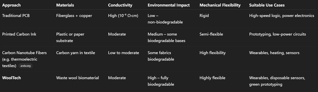

WoolTech uniquely combines full biodegradability, integrated structural substrate, and laser‑patterned electronics in a single wool‑based platform—a combination rarely found in existing smart textile research.
6. Engineering Integration: Best Practices & Challenges
6.1 Design for Laser Trace Patterns
Trace width and spacing must account for wool porosity and ink diffusion.
Test prototypes to calibrate laser power and speed for consistent conductivity.
Component pads must be reinforced—perhaps with small biodegradable resin or a firmer wool structure.
6.2 Compartmentalizing Electronics
Since traditional PCBs can’t be embedded, discrete ICs or microcontrollers must be mounted in a way that avoids physical stress on wool substrates—perhaps via biodegradable polymer “islands” or clip-in modules.
6.3 Power Delivery & Interconnects
Use conductive wool traces limited to low‑current signals.
For higher current needs (motors, displays), integrate detachable connectors—potentially natural conductive threads or interlocking wool pieces.
6.4 Environmental and Lifecycle Considerations
End‑of‑life: Being biodegradable, WoolTech boards can be composted or biodegraded.
Longevity: Coatings and finishes must protect against moisture and abrasion for wearables.
Scalability: Sourcing consistent waste wool and developing scalable laser processing are key challenges for mass adoption.
7. Possible Use Case: WoolTech Sensor Patch
An example development project for electronics engineers:
Process sheep‑wool into a flat panel (~50 × 50 mm).
Coat with conductive graphene/carbon-based ink.
Laser‑scribe a simple circuit for an LED, temperature sensor, and NFC or passive RF tag.
Mount a small temp sensor (e.g. thermistor), button cell sized biodegradable battery or RFID tag module.
Fold the panel into a patch, encapsulate in wool cover.
Wearable patch monitors temperature, LED signals, and communicates wirelessly via passive RFID coil coil.
All parts degrade over months, leaving only natural materials behind.
8. Opportunities & Future Directions
Improving Conductivity: Experiment with graphene oxide reduction, carbon nanotube impregnation, or metallic particle-free conductive polymers to lower resistance.
Integrating Energy Harvesters: Pair thermoelectric wool platforms or photovoltaic inks to power passive circuits.
Biocompatibility & Additives: Use antimicrobial finishes or dye-free wool for medical wearable prototypes.
Commercialization Path: Partner with textile labs and laser‑fabrication workshops to refine reproducibility and scale.
9. Prototype Roadmap for Engineers
Phase 1 – Lab Tests: Build test substrates, measure resistivity, mechanical flex, thermal endurance.
Phase 2 – Electronic Performance: Wire simple circuits, evaluate signal integrity and power limits.
Phase 3 – Wearable Integration: Design patches or fabric‐embedded modules and test on body movement.
Phase 4 – Environmental Stress Testing: Assess moisture, microbial exposure, UV, and wear over time.
Phase 5 – Field Application Trials: Deploy sensors in the field for durability and user‑feedback studies.
10. Why This Matters for Electronics Engineers
Circular resource design: Engineers can design electronics that avoid plastic and metals entirely—addressing sustainability at the material level.
Flexible prototyping: Laser-based patterning enables quick iteration without PCB fabrication.
Emerging green electronics trend: As regulators and markets grow conscious of e‑waste, WoolTech positions engineers ahead in eco-conscious electronics.
Integration with smart textiles: Combined with battery‑free textile systems, WoolTech offers a platform for future wearable-tech development.
11. Summary & Final Thoughts
WoolTech by Hinna Khan represents a bold departure from traditional electronics: using waste wool as both structure and circuit medium, patterned via laser, and yielding fully biodegradable devices. While performance currently suits low-power, flexible sensor systems rather than high-frequency or power-intensive circuits, the technology aligns perfectly with wearable electronics, rapid prototyping, green hardware, and educational applications.
For electronics project developers, WoolTech offers:
A structurally integral, natural substrate,
Low-barrier laser fabrication,
Biofriendly lifecycle,
Exciting potential for integration into textile and battery-free systems.
As the technology matures, expect further refinement in conductivity, resilience, and integration workflows—making WoolTech a material to watch for sustainable hardware innovation.
Engineer Checklist – Getting Started
Source waste wool and develop a standard cleaning/process pipeline.
Choose or formulate a conductive coating ink compatible with wool.
Calibrate laser cutting/patterning systems for trace formation.
Design sample circuits: sensor, LED, RFID or simple microcontroller.
Test mechanical robustness, electrical resistance, stretching/flex cycles.
Document biodegradation timeline and environmental testing data.
Closing thoughts: WoolTech heralds a new chapter in biomaterial electronics, where sustainable design meets functionality. It's an exciting opportunity for engineers to engage in low‑impact hardware innovation that pushes the boundaries of what “electronics” can be. Let me know if you'd like help designing a specific prototype or simulation workflow using WoolTech materials!
SERVICES
Peakingtech © 2025. · Shenzhen, China · Privacy Policy · Terms of Service
Contact Form
Metal Parts
Peakingtech® is a registered trademark of Peakingtech Co in the United States.
COMPANY
CONTACT