The Rise of Perovskite LED Technology: Revolutionizing Displays, Lighting, and Beyond
Discover the transformative potential of Perovskite LED (PeLED) technology in this in-depth article. Explore its advantages, recent advancements in efficiency and stability, challenges, and future applications in displays, lighting, and wearables as of June 2025. Learn how PeLEDs are revolutionizing optoelectronics with high color purity and low-cost processing.
PRODUCT DEVELOPMENT
JoeZ
6/7/20258 min read
In the ever-evolving world of optoelectronics, a new star has emerged: Perovskite Light-Emitting Diodes (PeLEDs). These innovative devices, leveraging the unique properties of perovskite materials, are poised to transform industries ranging from displays and lighting to wearable technology and visible light communication. In this comprehensive article, we’ll explore the fundamentals of PeLED technology, its advantages, recent advancements, challenges, and future prospects. By the end, you’ll understand why PeLEDs are being hailed as the next big thing in light-emitting technology.
What Are Perovskite LEDs?
Perovskite LEDs (PeLEDs) are a class of light-emitting diodes that use perovskite materials as their emissive layer to produce light. Perovskites are a family of materials with the chemical formula ABX₃, where:
A is a cation, such as cesium (Cs), methylammonium (MA), or formamidinium (FA);
B is a cation, typically lead (Pb) or tin (Sn);
X is a halide anion, such as chloride (Cl), bromide (Br), or iodide (I).
These materials can be organic-inorganic hybrids (e.g., CH₃NH₃PbBr₃) or all-inorganic (e.g., CsPbBr₃). One of the standout features of perovskites is their tunability: by adjusting the composition of A, B, and X, the bandgap—and thus the emission wavelength—can be precisely controlled, spanning the visible spectrum (blue, green, red) and even extending into the near-infrared region.
PeLEDs function similarly to other LEDs: electrons and holes are injected into the perovskite layer, where they recombine to emit photons (light). The color of the emitted light depends on the perovskite’s bandgap, making these devices incredibly versatile for applications requiring specific wavelengths, such as high-definition displays or energy-efficient lighting.
Why Perovskite LEDs Matter: Key Advantages
PeLEDs have captured the attention of researchers and industry leaders alike due to their remarkable properties, which offer several advantages over traditional technologies like organic LEDs (OLEDs) and quantum dot LEDs (QLEDs). Let’s break down these benefits:
1. High Color Purity and Tunability
Perovskites are renowned for their narrow emission bandwidths, with a full width at half maximum (FWHM) typically ranging from 5 to 40 nm. This results in exceptional color purity, which is crucial for applications like displays and lighting, where vibrant and accurate colors are essential. By tweaking the halide composition—using chloride for blue, bromide for green, and iodide for red—researchers can tune the emission across the entire visible spectrum, making PeLEDs highly versatile.
2. High Luminescence Efficiency
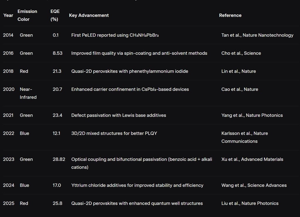
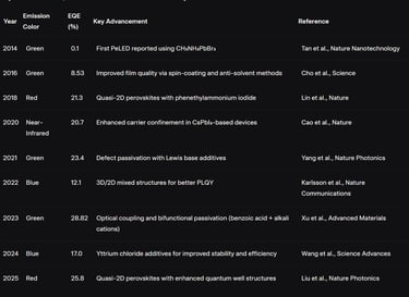
PeLEDs have achieved impressive external quantum efficiencies (EQEs), a measure of how efficiently injected electrons are converted into emitted photons. For green, red, and near-infrared PeLEDs, EQEs have surpassed 20%, with a record of 28.82% for green quasi-2D PeLEDs in 2023, thanks to optical coupling enhancements and defect passivation techniques. Even blue PeLEDs, which have historically lagged, reached an EQE of 17% in 2024, a significant milestone. Additionally, photoluminescence quantum yields (PLQY) in some 2D and quasi-2D perovskites approach 100%, indicating near-perfect light emission efficiency.
3. Cost-Effective and Simple Processing
Unlike traditional III-V semiconductor LEDs, which require complex and expensive fabrication processes, perovskites can be processed using low-cost, solution-based techniques such as spin-coating, blade-coating, and inkjet printing. This makes PeLEDs an economically viable option for large-scale production. Furthermore, their compatibility with flexible substrates opens the door to innovative applications, such as foldable displays and wearable devices.
4. Flexibility and Versatility
PeLEDs combine the best of both worlds: the flexibility and thinness of OLEDs and the color tunability of III-V LEDs. This makes them suitable for a wide range of applications, from high-resolution displays and energy-efficient lighting to emerging fields like visible light communication and biomedical imaging.
5. Environmental Potential
While lead in perovskites has raised toxicity concerns, studies suggest that its environmental impact is minimal compared to other materials, such as gold electrodes. A 2025 life cycle assessment of 18 PeLEDs found them to be eco-friendly and cost-competitive, especially if gold electrodes are replaced with less toxic alternatives like copper, aluminum, or nickel.
Recent Advancements in PeLED Technology
The past decade has seen rapid progress in PeLED technology, with breakthroughs in efficiency, stability, and novel applications. Let’s explore some of the most significant developments.
Efficiency Milestones
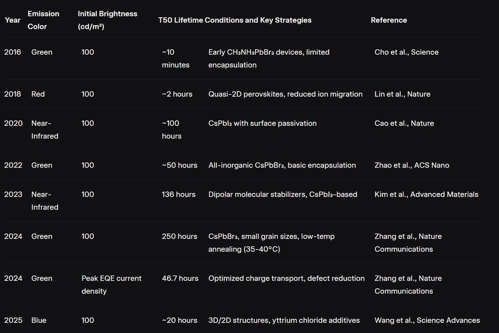
High EQEs Across the Spectrum: Green, red, and near-infrared PeLEDs have consistently surpassed 20% EQE. In 2023, green quasi-2D PeLEDs achieved a record EQE of 28.82% by using bifunctional passivators like Lewis base benzoic acid anions and alkali metal cations to reduce defects and enhance optical coupling. Red PeLEDs hit 25.8% EQE in 2025 with improved quantum well structures in quasi-2D perovskites.
Blue PeLED Breakthroughs: Blue PeLEDs, which have been a challenge due to their wide bandgap and emission quenching, reached an EQE of 17% in 2024. This was made possible by incorporating yttrium chloride additives and 3D/2D mixed structures, boosting the photoluminescence quantum yield to 49.7%.
Photon Recycling: Researchers have leveraged perovskites’ strong optical absorption and small Stokes shift to recycle trapped photons, significantly improving external efficiencies.
Stability Improvements
Stability has been a major hurdle for PeLEDs, but recent advancements have brought them closer to commercial viability:
Ultralong Lifetimes: Near-infrared PeLEDs achieved an operational lifetime (T50, the time for brightness to decay to 50% of its initial value) of 136 hours at 100 cd/m² in 2023, thanks to dipolar molecular stabilizers in CsPbI₃-based devices. This meets some commercial requirements for niche applications.
Green PeLEDs: In 2024, all-inorganic CsPbBr₃ PeLEDs demonstrated a T50 of 250 hours at 100 cd/m², achieved through small grain sizes and low-temperature annealing (35-40°C) to control crystal growth along the (110) plane, reducing defects.
Blue PeLEDs: While blue PeLEDs still lag, a 2025 study reported a T50 of 20 hours at 100 cd/m², a step forward enabled by 3D/2D structures and yttrium chloride additives.
Novel Structures and Applications
Quasi-2D Perovskites: These layered structures create quantum wells that enhance carrier confinement and luminescence efficiency. They’ve been particularly successful for red and green emissions, achieving EQEs of 25.8% at 680 nm in 2025.
Large-Area Devices: Researchers used L-methionine (NVAL) to inhibit phase segregation, enabling large-area (9.0 cm²) quasi-2D green PeLEDs with an EQE of 16.4% and luminance of 91,000 cd/m².
Micro-LEDs for Displays: Remote epitaxial growth of continuous perovskite films, using subnanometer graphene interlayers, has produced micro-LEDs with pixel sizes as small as 4 μm. These devices achieved 16.7% electroluminescence efficiency and a brightness of 400,000 cd/m², ideal for ultrahigh-resolution displays.
White PeLEDs: By coupling blue perovskite diodes with red perovskite nanocrystals, researchers created white PeLEDs with off-device quantum efficiencies exceeding 12% and brightness over 2,000 cd/m².
Flexible PeLEDs: The solution-processable nature of perovskites makes them ideal for flexible applications. For instance, a 2024 study showcased a wearable device—a smartwatch band—using a flexible PeLED display with vibrant green, red, and blue emissions, highlighting the potential for consumer electronics.
Light Management Innovations
To overcome efficiency bottlenecks, researchers have focused on light management:
Photon Recycling and Optical Design: By exploiting perovskites’ optical properties, such as tunable refractive indices and small Stokes shifts, trapped photons can be recycled, boosting external efficiencies.
Nanostructures: Moth-eye ZnO layers and anodic alumina membranes with nanodome and nanowire arrays have improved light outcoupling, achieving extraction efficiencies up to 73.6% and EQEs from 8.19% to 17.5%.
Challenges Facing PeLED Technology
Despite these advancements, several challenges must be addressed before PeLEDs can achieve widespread commercial adoption.
1. Stability and Lifetime
Current Limitations: PeLED lifetimes range from minutes to hundreds of hours, far below the 10,000-hour minimum for OLED displays or 50,000 hours for traditional semiconductor LEDs. For example, while near-infrared PeLEDs have reached 136 hours, blue PeLEDs struggle to exceed 20 hours.
Causes: Ionic migration, structural instability, and chemical degradation (due to moisture, oxygen, and joule heating) are major culprits. Organic cations like MA⁺ are hygroscopic, forming hydrated phases that release iodine gas and cause irreversible damage.
Blue PeLEDs: These devices suffer from poor photoluminescence efficiency, color instability, and emission quenching by interlayers, making them the least stable.
2. Efficiency Roll-Off
At high current densities (corresponding to high brightness), PeLED efficiency drops due to nonradiative Auger- and trap-assisted recombination and hole leakage into electron transport layers. This “efficiency roll-off” limits their use in high-brightness applications.
3. Toxicity Concerns
Lead, a key component in high-performance PeLEDs, raises environmental and health concerns. While its impact is considered minor, alternatives like tin-based perovskites are being explored, though they currently suffer from lower performance and stability. Additionally, replacing gold electrodes with less toxic materials like copper or nickel is recommended to further reduce environmental impact.
4. Scalability and Patterning
For display applications, high-resolution, full-color micro-LED arrays require precise patterning without degrading the perovskite films. Traditional methods like photolithography and etching can damage the material. Emerging techniques, such as bottom-up approaches (e.g., groove templates, patterned parylene films) and transfer printing, show promise but need refinement for large-scale production.
5. Device Integration
Integrating PeLEDs into traditional electronics or flexible platforms remains challenging. Advances in stamp preparation, heat treatment, and interface modulation are needed to ensure compatibility and reliability.
Future Prospects: Where PeLEDs Are Headed
The future of PeLEDs is bright, with researchers actively addressing the challenges outlined above. Here are some key directions for the technology:
1. Enhancing Stability
Encapsulation and Material Design: Advanced encapsulation techniques, robust interface modifications, and stable perovskite compositions (e.g., all-inorganic CsPbX₃) could extend lifetimes to commercial levels.
Photon Recycling: Leveraging photon recycling and nanostructured designs can mitigate degradation while improving efficiency.
2. Improving Efficiency
Light Management: Techniques like photon recycling, tailored optical properties, and nanostructured layers (e.g., distributed Bragg reflectors) can push external efficiencies closer to 100%.
Addressing Efficiency Roll-Off: Better carrier confinement and defect reduction strategies will help maintain efficiency at high brightness levels.
3. Advancing Blue PeLEDs
Blue PeLEDs are critical for full-color displays, but they lag in both efficiency and stability. Future efforts will focus on wide-bandgap perovskites, ligand engineering, and interfacial control to improve color stability and PLQY.
4. Sustainable Materials
Lead-Free Perovskites: Developing high-performance, stable tin-based perovskites could eliminate toxicity concerns.
Eco-Friendly Electrodes: Replacing gold with copper, aluminum, or nickel will reduce the environmental footprint of PeLEDs.
5. Scalability and New Applications
High-Resolution Displays: Non-destructive patterning techniques like nanoimprinting and transfer printing will enable high-resolution, full-color micro-LED arrays for displays.
Flexible and Wearable Devices: PeLEDs’ compatibility with flexible substrates makes them ideal for wearable electronics, such as smartwatch bands with vibrant displays, as demonstrated in recent studies.
Emerging Uses: PeLEDs could find applications in ultracompact lasers, ultrafast LEDs for visible light communication, and biomedical imaging, leveraging their high brightness and tunability.
6. Commercialization Goals
To compete with OLEDs and QLEDs, PeLEDs must achieve lifetimes exceeding 10,000 hours. Large-scale fabrication studies and research into nucleation/crystallization processes will be key to industrial adoption.
A Glimpse into PeLED Applications: Wearable Technology
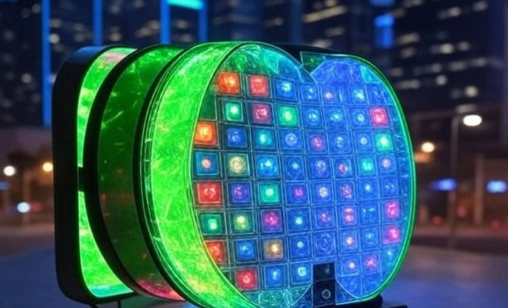
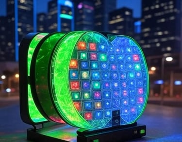
One of the most exciting applications of PeLEDs is in wearable technology. Imagine a smartwatch band that not only tells the time but also displays notifications, health data, or even decorative patterns using a flexible PeLED display. In 2024, researchers showcased such a device, utilizing all-inorganic CsPbBr₃ PeLEDs with low-temperature annealing for controlled crystal growth. The band emitted vibrant green, red, and blue light with high color purity, set against a futuristic cityscape, symbolizing the technology’s potential in consumer electronics. This application highlights PeLEDs’ flexibility, high efficiency, and ability to produce vivid colors, making them a game-changer for wearable devices.
Conclusion: The Dawn of a New Era in Optoelectronics
Perovskite LED technology is on the cusp of revolutionizing the optoelectronics industry. With their high color purity, tunable emission, impressive efficiencies, and low-cost processing, PeLEDs offer a compelling alternative to OLEDs and QLEDs. Recent advancements—such as EQEs exceeding 20%, ultralong lifetimes for near-infrared devices, and the development of micro-LEDs and flexible displays—demonstrate their immense potential. However, challenges like stability, efficiency roll-off, and scalability must be overcome to unlock their full commercial potential.
As of June 2025, the trajectory of PeLEDs is clear: with continued research into material design, light management, and sustainable practices, they could become the cornerstone of next-generation displays, lighting, and beyond. Whether it’s a foldable display, a wearable health monitor, or a high-speed communication system, PeLEDs are set to illuminate the future—literally and figuratively.
If you’re intrigued by the possibilities of PeLEDs, stay tuned for more updates as this technology continues to evolve. The future of light is brighter than ever, and perovskites are leading the way.
SERVICES
Peakingtech © 2025. · Shenzhen, China · Privacy Policy · Terms of Service
Contact Form
Metal Parts
Peakingtech® is a registered trademark of Peakingtech Co in the United States.
COMPANY
CONTACT