Liquid Metal‑Infused Vitrimer PCBs: A Self‑Healing, Reconfigurable Future
Discover how liquid metal-infused vitrimer circuit boards are revolutionizing electronics with self-healing, reconfigurable, and recyclable capabilities. This in-depth guide explores the science, engineering applications, and future potential of this groundbreaking technology for developers and engineers.
ELECTRONICS MANUFACTURING
JoeZ
7/2/20253 min read
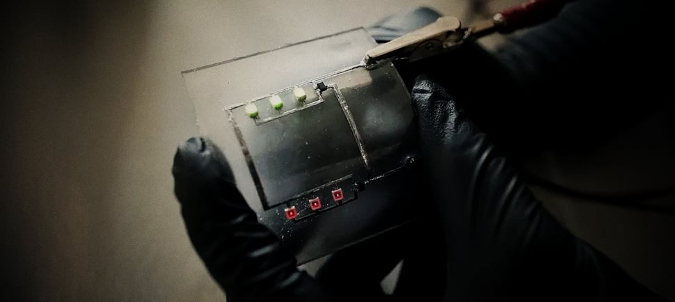
In a world grappling with ever‑mounting e‑waste, recent innovation from Virginia Tech could be a game‑changer for electronics developers and engineers. An April study showcased a printed circuit board (PCB) composite made of vitrimer—a dynamic polymer—infused with liquid metal droplets, delivering self‑healing, reconfigurable, and recyclable electronics that continue working even after serious damage.
Let’s break into the details, explore use cases, and consider implications for engineers shaping the future of resilient and sustainable electronics.
1. What is vitrimer, and why does it matter?
Traditional PCBs are cast in thermosetting plastics like epoxy, which offer mechanical rigidity but at the cost of flexibility and recyclability:
Thermosets = permanent, brittle, and unrecyclable
Vitrimers = dynamic, re-shapable, reparable, and recyclable
Vitrimers feature covalent cross-links that reorganize under heat—allowing boards to be reshaped, repaired, or chemically recycled. By applying heat, the material softens, enabling structural reconfiguration and even full component recovery later.
Why this matters for engineers:
Enables prototyping with "morphable" boards
Mechanical damage can be healed on‑board
Facilitates thermoplastics‑like reflow repair on embedded boards
Simplifies e‑waste handling and material reclamation
2. Liquid metal: stretchy yet conductive
The Johns Hopkins research group added ~5% liquid metal droplets (e.g. eutectic Ga‑In alloy) into the vitrimer matrix, achieving a ~2× increase in tensile strain before failure . The liquid metal core offers:
Metal-level conductivity even when stretched or cut
Autonomous redistribution: breaks allow droplets to flow and reconnect paths
Intrinsic redundancy: microdroplets form overlapping conductive networks
This is more than proof-of-concept: a self-healing, functional trace is possible—without additional healing agents or catalysts.
3. Lab-Scale Testing: Torture‑Testing
Virginia Tech researchers used a universal testing machine to simulate strain and compressive loading. Remarkably, post-damage heating:
Restored mechanical integrity
Re-established circuit function
In some test scenarios, boards subjected to cuts and delamination were reheated to recover trace continuity and mechanical strength.
4. Towards sustainable electronics
The PCB composite can be fully recycled via alkaline hydrolysis, reclaiming embedded LEDs, liquid metal, and PCR resin. With global e-waste projected to exceed 82 million tonnes by 2030—with only ~20% recycled—the environmental impact cannot be overstated.
For engineers:
Design for circularity becomes feasible
Boards can be repurposed and remanufactured
Regulatory and sustainability impact: less landfill, fewer hazardous leachates
5. Broader Liquid‑Metal PCBs: BiLiSC & others
This isn’t just one-off innovation. Singapore’s National University introduced BiLiSC, a bilayer liquid‑metal/elastomer conductor:
Stretchable to 22× original length, minimal conductivity drop
Instantaneous micro‑crack healing via microdroplet flow
Applied in sensors, antennas, heaters and soft robotics
More generally, gallium-based alloys like EGaIn and Galinstan are being explored across the board for printable, patternable, self-healing electronics.
6. Engineering Challenges & Practical Considerations
While promising, several hurdles remain:
Integration with SMDs: Traditional PCBs rely on soldered joints—adapting these resins/liquid-metal systems to meet temperature and pad geometry specs requires innovation.
Trace resolution: Current droplets form features at ~200 μm resolution—sufficient for low-frequency interconnects, possibly limiting high‑density designs .
Aging & fatigue: Long-term stability, microdroplet oxidation (oxide skins), and mechanical wear need to be thoroughly tested.
Thermal & electrical performance: Liquid metals behave differently thermally. Design rules for IR profiling, heat dissipation, and EMI shielding need revisiting.
Regulatory/commercial materials: Sourcing Ga‑In alloys at scale, material safety, RoHS, and integration into current manufacturing flows will be key.
7. Potential Use Cases: Where this shines
Wearables & e-skin
Flexible sensors that self-repair under strain
Ultra-comfortable bandages and human-machine interfaces
Soft robotics
Strain-rated flexible circuits that heald after impact
Printed antenna arrays on soft substrates
Rapid prototyping & configurability
Boards that can be morphologically edited post-production
Functionally reconfigurable test jigs
E-waste reduction & smart recycling
Boards that are more than disposable
Reclaimed circuits and components, on‑demand
8. Engineering Roadmap
For teams eyeing implementation:
Material sourcing: Confirm availability of Ga‑In and vitrimer blends
Circuit design: Use larger traces and embedded pads for multi‑layer setups
Manufacture: Explore extrusion, screen printing, microdispensing
Evaluation: Measure conductivity, cycle‑to-failure, strain vs. functional loss
Failure & repair testing: Simulate cuts, reheating recovery, trace continuity mapping
Environmental testing: Heat/humidity stress, aging, wash cycles
9. The road ahead: a frank evaluation
Pros:
Enables self‑healing PCBs
Offers recyclability and configurable functionality
Great for prototyping, wearables, robotic systems, and sensors
Cons:
Limited miniaturization vs. FR4
Material compatibility (thermal, electrical) remains under study
Scale‑up and standards compliance issues pending
10. Final Thoughts
Liquid metal‑infused vitrimer composites herald a new class of resilient, healable, and recyclable electronics. Engineers now have a toolkit to fabricate boards that mend themselves, morph shape, and can be chemically recycled—far from the throw‑away PCBs of the past.
For applications where flexibility, resilience, and sustainability intersect—from wearable medical sensors to evolving robotics—this approach is pivotal. While not replacing high‑density rigid PCBs, it unlocks applications previously impossible.
As the materials mature, expect startups, standards, and design tools to adapt quickly. Graduates of soft robotics labs and print‑electronics programs should track this space closely. If you're modeling next-gen devices, it's time to wet the ends of your traces with liquid metal—and build toward self‑healing, earth‑friendly circuitry.
Further Reading & References
Original Advanced Materials study: self‑healing PCB via vitrimer + Ga‑In alloy
UN e-waste forecast 2030, recycling stats
NUS BiLiSC liquid‑metal bilayer stretchable conductors
Review on gallium-based liquid metals in flexible electronics
SERVICES
Peakingtech © 2025. · Shenzhen, China · Privacy Policy · Terms of Service
Contact Form
Metal Parts
Peakingtech® is a registered trademark of Peakingtech Co in the United States.
COMPANY
CONTACT