How Many Processes Are Involved in Electronics Manufacturing?
Electronics manufacturing is a complex, multi-step process that transforms an initial concept into a fully functional product. Whether it’s a simple circuit board or a high-tech consumer device, manufacturing involves a series of interconnected processes, each playing a crucial role in ensuring product quality, functionality, and reliability.
1/31/202513 min read
Introduction
Electronics play a vital role in modern life, powering everything from simple household gadgets to sophisticated consumer devices. Electronics manufacturing is a complex, multi-step process that transforms an initial concept into a fully functional product. Whether it’s a simple circuit board or a high-tech consumer device, manufacturing involves a series of interconnected processes, each playing a crucial role in ensuring product quality, functionality, and reliability.
Understanding the key stages of electronics manufacturing is essential for product developers, engineers, and business owners. From initial design and prototyping to large-scale production and final quality testing, every step requires meticulous planning, technical expertise, and strict quality control measures. Additionally, factors such as component sourcing, supply chain management, and compliance with industry standards further influence the efficiency and cost-effectiveness of the entire process.
In this article, we will break down the various processes involved in electronics manufacturing from the perspective of an electronics manufacturer, highlighting the critical steps required to bring an electronic product from concept to market. By understanding these steps, companies can make informed decisions to optimize production, reduce costs, and improve product performance.
Key Stages in Electronics Manufacturing
Electronics manufacturing is a structured, multi-phase process that ensures a product moves from an initial idea to a market-ready device. Each stage involves specific technical and operational procedures that contribute to the final product’s quality, performance, and cost-efficiency. Below are the key stages involved in electronics manufacturing:
A. Design & Prototyping
Product Concept and Requirements Definition
The foundation of any electronic product begins with careful planning and design. This stage ensures that the product meets all functional requirements while being optimized for cost-effective manufacturing. The process starts with defining the product concept and requirements. This involves identifying the target market and the intended use of the product, as well as establishing key specifications such as power requirements, connectivity, and user interface design.
Electronic Circuit Design & PCB Layout
Once the requirements are clear, the next step is electronic circuit design and PCB layout. Engineers use Electronic Design Automation (EDA) tools like Altium Designer, Eagle, or KiCad to create circuit schematics. During this phase, factors such as signal integrity, thermal management, and manufacturability are carefully considered to ensure optimal performance.
Component Selection & Bill of Materials (BOM) Creation
Component selection and Bill of Materials (BOM) creation follow next. Choosing the right electronic components is crucial for balancing performance, cost, and availability. A BOM is then created to list all components required for manufacturing, ensuring efficient procurement and production planning.
Prototyping & Design Validation
Finally, the design undergoes prototyping and validation. Small-scale prototypes are produced for initial testing, allowing engineers to verify functionality and identify any design flaws. Functional verification is conducted to debug issues before moving forward with large-scale manufacturing, ensuring a reliable and well-optimized product.


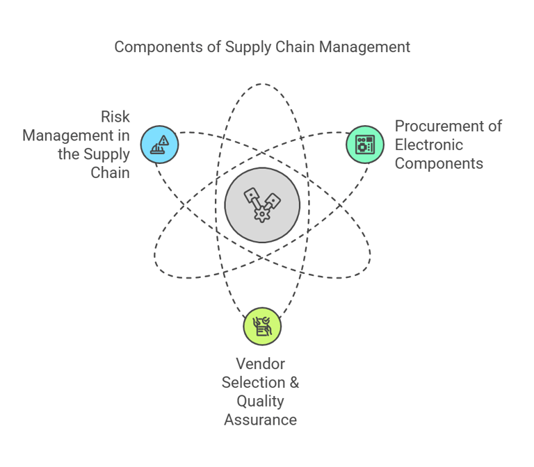
B. Sourcing & Supply Chain Management
Efficient sourcing of components is crucial for cost control and production stability in electronics manufacturing. A well-managed sourcing strategy must balance multiple factors including component costs, supplier reliability, lead times, and quality consistency. Manufacturers need to maintain relationships with multiple qualified suppliers to mitigate supply chain risks and avoid production disruptions due to component shortages. Strategic decisions about component selection during the design phase can significantly impact long-term manufacturing costs, as choosing widely available components from reputable manufacturers helps ensure stable pricing and reliable supply. Additionally, careful inventory management and demand forecasting enable companies to optimize their component purchasing, avoiding both costly stockouts and excess inventory while maintaining the flexibility to respond to market changes or unexpected demand spikes.
Product Concept and Requirements Definition
Efficient sourcing of components is crucial for maintaining cost control and ensuring production stability in electronics manufacturing. The process begins with the procurement of electronic components, including microcontrollers, resistors, capacitors, integrated circuits (ICs), and other essential parts. Manufacturers must carefully evaluate suppliers based on factors such as quality, pricing, and reliability to secure the best components for production.
Vendor Selection & Quality Assurance
Vendor selection and quality assurance play a vital role in reducing supply chain risks. Partnering with verified suppliers helps ensure a consistent supply of high-quality components while minimizing disruptions. Additionally, thorough certifications and compliance checks are conducted to confirm that all parts meet industry standards and regulatory requirements.
Risk Management in the Supply Chain
Risk management within the supply chain is another critical aspect of sourcing. Manufacturers must proactively address potential challenges such as component shortages, counterfeit risks, and long lead times. Establishing relationships with multiple suppliers and maintaining backup sources helps mitigate these risks, ensuring a steady and reliable flow of materials for production.

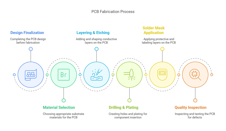
C. PCB Fabrication
The PCB fabrication process is a critical manufacturing phase that transforms a circuit design into a physical board. This multi-step process requires precision engineering and strict quality control to ensure reliable electronic components.
PCB Substrate Material Selection The foundation of any PCB begins with selecting the appropriate substrate material. FR4, a glass-reinforced epoxy laminate, is the most common choice due to its excellent balance of cost and performance. It offers good electrical insulation and mechanical strength at reasonable prices. For high-frequency applications, Rogers materials provide superior signal integrity and lower dielectric losses, though at a higher cost. Flexible PCBs, made from polyimide or similar materials, enable designs that can bend or fold, ideal for compact devices or applications requiring dynamic movement.
Layering & Etching Process The layering process begins with copper-clad laminate sheets. For multilayer boards, multiple layers are precisely aligned and bonded together using prepreg (pre-impregnated) material under heat and pressure. The etching process uses photolithography, where a photoresist layer is applied and exposed to UV light through a mask containing the circuit pattern. Unwanted copper is then chemically etched away, leaving only the desired circuit traces. This process requires careful control of chemical concentrations and timing to maintain trace integrity.
Drilling, Plating, and Solder Mask Application Computer-controlled drilling machines create precise holes for component mounting and vias. These holes undergo electroless copper plating, followed by electroplating to ensure reliable electrical connections between layers. The solder mask, typically green but available in various colors, is applied to protect copper traces from oxidation and prevent solder bridges during assembly. The silkscreen layer adds component identifiers, polarity markers, and other essential information for assembly and maintenance. Proper alignment of these layers is crucial for manufacturing success.
Quality Inspection & Electrical Testing Quality control employs multiple inspection methods. Automated Optical Inspection (AOI) systems use high-resolution cameras and pattern matching algorithms to detect visual defects like broken traces, copper shorts, or incorrect hole sizes. Flying probe testers or bed-of-nails fixtures perform electrical continuity testing to verify connections between points. Advanced testing may include impedance testing for high-speed circuits and microsection analysis to verify internal layer quality. Any boards failing these tests are marked and removed from production.

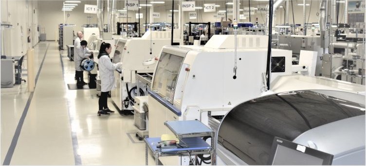
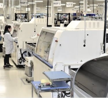
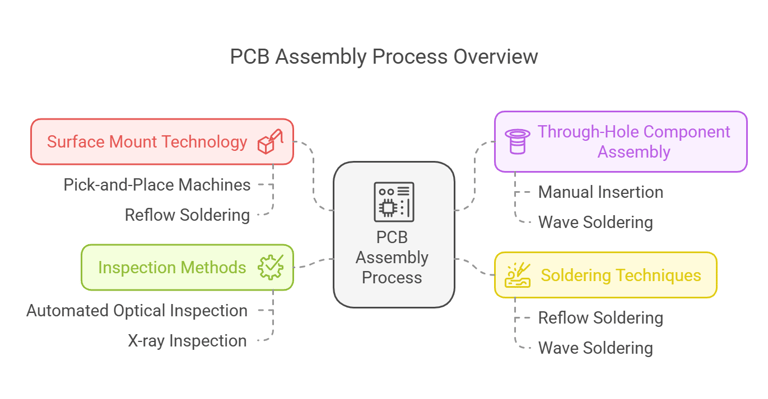
D. PCB Assembly (PCBA)
PCB Assembly transforms a bare circuit board into a functional electronic assembly through precise component placement and soldering processes. This stage combines automated and manual techniques to achieve high-quality, reliable electronic assemblies.
Surface Mount Technology (SMT) Process Modern electronics rely heavily on SMT for its efficiency and miniaturization capabilities. The process begins with applying solder paste through a stencil onto the PCB's surface mount pads. High-speed pick-and-place machines, capable of placing thousands of components per hour, use computer vision and precision robotics to position components as small as 0201 (0.6 x 0.3mm) or smaller. These machines maintain placement accuracy within 0.05mm while handling various component types including resistors, capacitors, ICs, and specialized packages. Component feeders automatically supply parts from tape reels, tubes, or trays, ensuring continuous production flow.
Through-Hole Component Assembly Through-hole assembly remains crucial for components requiring mechanical strength or high power handling. Components such as connectors, large capacitors, and transformers are inserted either manually by skilled operators or using automated insertion equipment. Manual assembly requires careful attention to component polarity and orientation. Automated insertion machines use component verification systems to prevent errors and maintain consistent insertion force. The leads are then clinched (bent) to hold components in place before soldering, ensuring mechanical stability.
Reflow Soldering & Wave Soldering Reflow soldering uses precisely controlled temperature profiles with multiple zones: preheat, soak, reflow, and cooling. The profile must accommodate the thermal requirements of all components while preventing issues like tombstoning or solder beading. Typical peak temperatures reach 230-250°C depending on solder composition. Wave soldering, used for through-hole components, passes boards over a standing wave of molten solder. The process requires careful control of wave height, temperature, and conveyor speed. Selective soldering offers an alternative for mixed-technology boards, precisely applying solder to specific through-hole locations while avoiding nearby SMT components.
Automated Optical Inspection (AOI) & X-ray Inspection Quality control employs sophisticated inspection technologies. AOI systems use multiple cameras and lighting angles to detect issues such as missing components, wrong polarity, insufficient solder, or excess solder. Machine learning algorithms help identify defects while minimizing false positives. X-ray inspection becomes crucial for Ball Grid Array (BGA) components and other hidden solder joints, allowing inspection of solder ball formation, void content, and bridge detection. Advanced X-ray systems provide both 2D and 3D imaging capabilities, enabling detailed analysis of internal structures and solder joint quality.

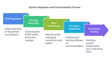
E. System Integration & Final Assembly
System integration marks the crucial final phase where individual PCB assemblies are transformed into complete, functional products. This stage requires careful attention to both mechanical and electrical integration while ensuring the final product meets all performance and reliability requirements.
Housing/Casing Assembly The housing assembly process involves careful integration of the PCBA into its final enclosure. This includes proper positioning of mounting points, thermal considerations for heat dissipation, and electromagnetic interference (EMI) shielding when required. Design features such as snap-fits, bosses, and screw posts must align precisely with the PCBA mounting holes. Gaskets and seals are installed for products requiring specific IP (Ingress Protection) ratings against dust and water. The assembly process must account for adequate clearance around components while maintaining a compact form factor. Special attention is paid to areas where user interaction occurs, such as button mechanisms, display windows, and connector openings.
Wire Harnessing & Cable Connections Wire harness assembly involves creating organized bundles of cables that connect various system components. Each cable is cut to precise lengths, stripped, and terminated with appropriate connectors. Color coding and labels ensure correct assembly and future serviceability. Strain relief mechanisms prevent mechanical stress on solder joints and connectors. Cable routing considers factors such as signal interference, bend radius limitations, and accessibility for maintenance. For RF applications, special attention is paid to antenna cable routing and shielding to maintain signal integrity. Wire gauge selection must account for current requirements and voltage drop considerations.
Firmware Installation & Software Programming The programming phase involves loading firmware onto microcontrollers, processors, and programmable devices. This often uses specialized programming fixtures or In-System Programming (ISP) interfaces. Version control systems ensure correct firmware variants are installed for different product models or configurations. Security features such as encryption keys or authentication codes are programmed when required. Initial configuration parameters are set according to product specifications. Some systems may require calibration data to be stored in non-volatile memory. The programming process includes verification steps to confirm successful code loading and basic functionality.
Functional & Performance Testing Comprehensive testing verifies proper operation of the complete system. Automated test equipment runs through predefined test sequences checking all product functions. This includes:
Power consumption measurements across different operating modes
Communication interface verification (USB, Ethernet, WiFi, Bluetooth, etc.)
Sensor calibration and performance validation
User interface testing including displays, buttons, and indicators
Environmental testing under specified temperature and humidity conditions
EMC (Electromagnetic Compatibility) testing for regulatory compliance
Burn-in testing at elevated temperatures to identify early failures
Audio/visual testing for products with multimedia capabilities
Quality assurance procedures document all test results for traceability. Products meeting all specifications are then prepared for packaging, including application of required labels, serial numbers, and regulatory markings. Final inspection ensures cosmetic quality and completeness of all included accessories before the product is packaged for shipping.
The success of system integration relies heavily on well-defined processes, trained personnel, and proper test equipment. Modern manufacturing facilities often implement real-time tracking systems to monitor yield rates and identify potential process issues quickly. This data-driven approach helps maintain high quality standards while optimizing production efficiency.

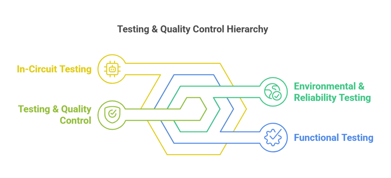
F. Testing & Quality Control
Testing and quality control represent essential phases in electronics manufacturing that ensure products meet stringent performance, reliability, and safety requirements. These processes employ multiple testing methodologies at different stages to catch defects early and verify compliance with specifications.
In-Circuit Testing (ICT)
ICT provides comprehensive electrical verification of assembled PCBs using specialized bed-of-nails fixtures. This automated testing process includes:
Component presence and orientation verification
Passive component measurements (resistance, capacitance, inductance)
Semiconductor junction testing for diodes and transistors
Power and ground continuity testing
Short circuit detection between adjacent nets
Analog signature analysis for complex components
The test fixtures use spring-loaded pins that make contact with designated test points on the PCB. Modern ICT systems can test thousands of points in seconds, providing detailed diagnostic information for any failures. Test programs are optimized to balance coverage with test time, and fixtures are designed to ensure reliable contact without damaging components or board surfaces.
Functional Testing (FCT)
Functional testing evaluates the product under actual operating conditions to verify real-world performance. This includes:
Power-up sequence verification
Current consumption measurement in various operating modes
Communication interface testing (USB, Ethernet, wireless)
Signal integrity analysis at critical circuit points
Software/firmware operation verification
User interface testing (displays, buttons, indicators)
Performance measurements (speed, accuracy, response time)
Custom test fixtures often incorporate product-specific interfaces and automated test sequences. Test results are logged for traceability and statistical analysis. Failed units undergo detailed diagnosis to identify root causes and drive continuous improvement in design and manufacturing processes.
Environmental & Reliability Testing
Environmental and reliability testing subjects products to stress conditions to verify robustness and regulatory compliance:
Temperature Testing:
Thermal cycling between specified temperature extremes
High-temperature operation testing
Cold start verification
Thermal shock resistance
Humidity Testing:
Operation under high humidity conditions
Moisture resistance verification
Condensation testing
Mechanical Testing:
Vibration testing at specified frequencies and amplitudes
Drop testing for portable devices
Mechanical shock resistance
Connector insertion/removal cycle testing
EMI/EMC Testing:
Radiated emissions measurements
Conducted emissions testing
Immunity to external interference
Electrostatic discharge (ESD) testing
Power supply transient testing
Reliability testing often includes accelerated life testing to predict long-term reliability. Statistical analysis of test results helps establish mean time between failures (MTBF) and other reliability metrics. All testing must comply with relevant industry standards (IEC, UL, CE, etc.) and regulatory requirements for the target markets.
Documentation and traceability are maintained throughout the testing process, including:
Test procedures and acceptance criteria
Calibration records for test equipment
Failure analysis reports
Corrective action documentation
Statistical process control (SPC) data
Compliance certificates
Modern testing facilities often implement automated data collection and analysis systems to identify trends and potential issues before they become significant problems. This data-driven approach enables continuous improvement in both product design and manufacturing processes.

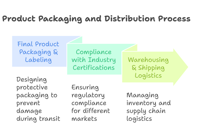
G. Packaging & Logistics
The packaging and logistics phase ensures products reach customers safely while maintaining compliance with regulatory requirements and efficient supply chain management.
Final Product Packaging & Labeling
Product packaging involves multiple layers of protection and information:
Primary Packaging:
Custom-molded foam inserts to prevent movement and absorb shock
Anti-static bags for electronics protection
Moisture barrier bags with desiccants for humidity-sensitive components
Protective films for displays and cosmetic surfaces
Product Identification:
Serial number tracking with both human-readable and barcode formats
Manufacturing date codes
Product model and revision information
Regulatory compliance marks (CE, FCC, UL, etc.)
RoHS and WEEE symbols where applicable
Country of origin labeling
QR codes linking to product documentation
Package Contents:
User manuals and quick start guides
Warranty cards and safety information
Required accessories and cables
Software installation media if applicable
Customer support contact information
Compliance with Industry Certifications
Regulatory compliance requires comprehensive documentation and testing:
Safety Certifications:
UL/CSA certification for North America
CE marking for European markets
CCC certification for China
PSE marking for Japan
Other region-specific safety approvals
Environmental Compliance:
RoHS verification of component materials
REACH compliance documentation
Energy efficiency certifications
Packaging material recyclability
Battery disposal regulations
Documentation Requirements:
Test reports from accredited laboratories
Technical construction files
Declaration of Conformity
Material safety data sheets
Environmental impact assessments
Product lifecycle documentation
Warehousing & Shipping Logistics
Supply chain management encompasses multiple aspects:
Inventory Management:
Real-time tracking of finished goods
First-in-first-out (FIFO) stock rotation
Serialized inventory control
Automated warehouse management systems
Climate-controlled storage for sensitive components
Distribution Planning:
Regional distribution center allocation
Transportation mode selection (air, sea, land)
Customs documentation preparation
Export/import compliance
Insurance coverage
Quality Control:
Pre-shipment inspections
Package drop testing
Environmental exposure monitoring
Transportation condition logging
Receipt verification procedures
Cost Optimization:
Bulk shipping arrangements
Container utilization planning
Route optimization
Third-party logistics partnerships
Just-in-time delivery coordination
The success of packaging and logistics operations relies on careful planning and coordination between manufacturing, quality control, and distribution teams. Modern systems employ advanced tracking technologies and data analytics to optimize efficiency and maintain product quality throughout the distribution chain. This includes:
RFID tracking for inventory management
Real-time shipment monitoring
Automated warehouse systems
Predictive analytics for demand planning
Digital documentation systems
Blockchain technology for supply chain transparency
Special consideration is given to handling requirements for sensitive electronic components, including:
Temperature and humidity monitoring during transit
Shock and vibration logging
Special handling instructions for carriers
Emergency response procedures
Return merchandise authorization (RMA) processes

Advanced & Emerging Manufacturing Processes
As electronics manufacturing continues to evolve, emerging technologies and advanced production techniques are reshaping the industry. These innovations enhance efficiency, reduce costs, and improve product quality. Below are some of the most significant advancements in modern electronics manufacturing.
A. Automation & Industry 4.0 in Electronics Manufacturing
The integration of automation and digital technologies—often referred to as Industry 4.0—has revolutionized manufacturing by improving efficiency and reducing human error.
Smart Factories & IoT Integration
Use of interconnected IoT-enabled sensors and devices for real-time monitoring.
Predictive maintenance using AI and big data to reduce downtime.
Cloud-based manufacturing execution systems (MES) for centralized control.
Robotics & Automated Assembly Lines
High-speed robotic arms for precision placement of components.
AI-powered automated optical inspection (AOI) for quality control.
Cobots (collaborative robots) working alongside human operators to improve production efficiency.
Digital Twins & Simulation
Virtual replicas of manufacturing processes allow real-time simulation and troubleshooting.
Enables rapid identification of bottlenecks and optimization of production workflows.
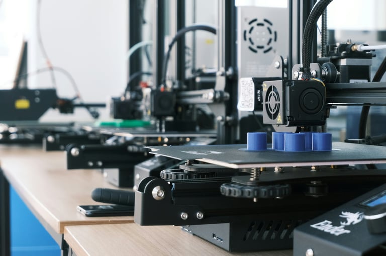
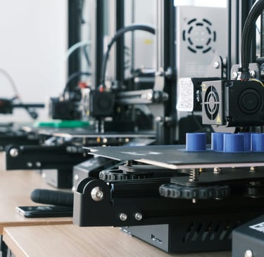
B. 3D Printing for Rapid Prototyping & Production
Additive manufacturing (3D printing) is transforming electronics development by enabling rapid prototyping and, in some cases, direct production of complex electronic components.
Rapid PCB Prototyping
3D-printed circuit boards reduce the time required to develop and test new designs.
Enables quick design iterations without waiting for traditional PCB fabrication.
Printed Electronics & Flexible Circuits
Conductive inks allow for printed circuit patterns on flexible substrates.
Used in wearable electronics, RFID tags, and flexible displays.
On-Demand Custom Parts & Enclosures
3D printing enables customized casings, heat sinks, and mechanical parts.
Reduces dependency on traditional injection molding for low-volume production.
C. AI-Driven Quality Control & Predictive Maintenance
Artificial intelligence (AI) and machine learning are transforming quality control and maintenance processes in electronics manufacturing.
AI-Powered Defect Detection
Machine vision systems analyze solder joints, component placement, and PCB defects.
AI continuously improves accuracy by learning from past inspection data.
Predictive Maintenance for Equipment
AI predicts machinery failures before they happen, reducing unplanned downtime.
IoT sensors collect data on vibration, temperature, and operational patterns.
Automated Supply Chain Optimization
AI-driven demand forecasting improves inventory management.
Reduces waste by optimizing component sourcing and logistics.
D. Advanced Materials & Miniaturization
New materials and techniques are enabling the production of smaller, more powerful, and more efficient electronic devices.
Use of Advanced Semiconductor Materials
Adoption of Gallium Nitride (GaN) and Silicon Carbide (SiC) for high-performance power electronics.
Enables energy-efficient, high-speed devices with reduced heat generation.
Miniaturization & High-Density Interconnects (HDI) PCBs
Advanced PCB fabrication techniques allow more components in smaller spaces.
Used in modern smartphones, wearables, and IoT devices.
Flexible & Stretchable Electronics
Integration of ultra-thin, bendable circuits for wearable tech and medical devices.
Enables the development of smart textiles and electronic skin applications.
E. Sustainable & Green Manufacturing Innovations
With increasing global focus on sustainability, electronics manufacturers are adopting greener practices to reduce waste and energy consumption.
Eco-Friendly PCB Manufacturing
Use of biodegradable PCB substrates and non-toxic etching processes.
Recycling and reusing materials to minimize electronic waste (e-waste).
Energy-Efficient Production Lines
Implementation of solar- and wind-powered manufacturing facilities.
AI-driven energy management systems optimize power usage.
Right-to-Repair & Circular Economy Initiatives
Designing products for easier repair, reducing landfill waste.
Encouraging modular components and extended product lifespans.
Conclusion
Advanced and emerging manufacturing processes are reshaping the electronics industry, enabling greater automation, efficiency, and sustainability. As technologies like AI, 3D printing, and Industry 4.0 continue to develop, companies that adopt these innovations will gain a competitive edge by reducing costs, improving quality, and accelerating product development.
SERVICES
Peakingtech © 2025. · Shenzhen, China · Privacy Policy · Terms of Service
Contact Form
Metal Parts
Peakingtech® is a registered trademark of Peakingtech Co in the United States.
COMPANY
CONTACT