The Dawn of Hybrid Electronic‑Photonic‑Quantum Chips
Discover how the world’s first hybrid electronic‑photonic‑quantum chip is revolutionizing the electronics industry. This in-depth article explores new opportunities for product innovation, manufacturing, and competitive advantage—essential reading for project leaders, decision-makers, and engineers driving the future of semiconductors.
JoeZ
7/20/20254 min read
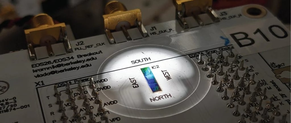
On July 18, 2025, SciTechDaily highlighted a groundbreaking chip: the world’s first hybrid semiconductor that unites electronic, photonic, and quantum components on a standard 45 nm CMOS platform. This milestone, detailed in Nature Electronics, brings together:
Quantum light sources: microring resonators generating correlated photon pairs.
On‑chip photonics: waveguides, microrings, photodiodes.
Control electronics: CMOS logic, photodiode feedback loops, heaters.
With 12 parallel quantum light sources on chip, each actively stabilized in real time via integrated control logic, this represents a leap toward scalable quantum devices.
For electronics companies, this convergence opens transformational opportunities across technology, products, and markets. Let’s unpack how.
1. Accelerated Entry into Quantum Photonics
🔹 Seamless Transition with CMOS
This chip's heritage is pure CMOS: 45 nm standard process, co‑developed with GlobalFoundries and Ayar Labs. For electronics firms, that’s a boon:
Lowers the barrier to mass‑custom silicon with minimal foundry adaptations.
Allows rapid prototyping and scaling without exotic processes.
Moves quantum photonic design from academic labs to state-of-the-art fabs.
🔹 Integrated Feedback & Control
Embedding photodiode-based feedback loops and on-chip heaters offers robust real-world stability—critical for transition from lab prototypes to manufacturable, high-volume products.
🔹 Building Modular “Quantum Light Factories”
Arrays of microrings form compact modules (~1 mm²) delivering stable photon streams. These can be scaled:
Tileable architectures for larger quantum systems.
Modular design enabling low-risk incremental integration into classical hardware.
2. New Product Categories & Value-Added Offerings
🔹 Quantum Communication & Security
Photon sources on CMOS pave the way for:
Quantum Key Distribution (QKD) modules in existing hardware.
Secure point-to-point channels for governments, finance, and data centers.
On-chip entangled photon sources, ready for quantum-safe encryption.
🔹 Quantum Sensing & Timing
Photon pairs enhance capabilities in:
High-precision sensors: LiDAR, gyros, magnetometers.
Optical clocks & metrology, leveraging quantum correlations for ultra-stable signals.
Resilient architectures through optical isolation.
🔹 Integrated Photonic AI and Interconnects
Photonics shines in bandwidth and energy efficiency:
On-chip optical interconnects for neuromorphic and AI accelerators.
Co‑packaging photonic I/O and photon sources with classical compute.
Enabling ultra-fast coherent interconnects far beyond electrical bottlenecks.
3. Manufacturing & Ecosystem Momentum
🔹 Foundry Collaboration & Standardization
Existing foundries adapting photonic modules set the stage for:
Standardized PDKs for photonic-electronic-quantum design (similar to RISC-V).
Economy of scale and widening ecosystem participation.
Tempest for new business models in fabless semiconductor strategies.
🔹 Rise of Hybrid Systems-Level Engineering
Creating such chips calls for multidisciplinary teams:
Integrated design combining RF engineers, photonic experts, control electronics, and QC scientists.
New EDA toolchains and multidisciplinary co-design flows.
Platforms for end-to-end system development (design to testing).
🔹 Supply Chain Expansion
New value chains emerge:
Specialized packaging: ultra-precise optical alignment.
Test equipment capable of quantum diagnostics and photonic characterization.
EDA & IP providers for optical waveguide synthesis and resonator analysis.
4. Strategic Shifts & Competitive Advantage
🔹 First-Mover Leadership
Early hybrid chip deployment can offer:
Unique selling propositions for defense, telecom, security.
Leadership in emerging quantum standards, steering industry roadmaps.
Attraction of strategic partnerships and public funding (e.g., Future of Semiconductors, Packard Foundation).
🔹 Market Ecosystem Sy energies
Photonics firms (e.g., Ayar Labs, PsiQuantum) are scaling CMOS-compatible designs. Electronics companies can:
Acquire startups with optical/module IP.
Spin off internal photonic divisions.
Launch joint ventures for hybrid IC design and integration.
🔹 Geopolitical & National Tech Leadership
As nations race to lead quantum tech, domestically accessible CMOS photonic chips:
Strengthen sovereignty in strategic semiconductor technologies.
Position electronics companies as key public–private strategic partners.
5. Roadblocks & R&D Imperatives
🔹 Thermal Management
Maintaining microring resonance demands:
Active temperature stabilization (on-chip heaters).
Overall thermal control in packaging and system deployment.
🔹 Yield & Fabrication Tolerances
Photonics tolerates fewer fluctuations; feedback loops help, but:
Tight process controls are essential.
Feedback-heavy designs may raise failure rates—fabrication variability must be mitigated.
🔹 Optical-Electrical Interface
Designers must engineer:
Extreme-low-loss waveguide-to-fiber or chiplet couplers.
Isolation of optoelectronic cross-talk.
High-speed drivers and detectors matched photonics performance.
🔹 EDA Tools & Workflows
Photonics demand new support:
Accurate simulation of photonic circuits, thermal effects, quantum behavior.
Verification tools for hybrid analog/digital/optical/quantum systems.
6. Path Forward & Tactical Steps
To capitalize on hybrid chips, electronics companies should consider:
Invest in R&D: Integrate leaders in photonic design and QC measurement.
Establish pilot lines: Co-locate photonic test facilities with CMOS fabs.
Forge partnerships: Collaborate with academic centers and startups (e.g., Ayar Labs, PsiQuantum).
Develop toolchains: Customized CAD and thermal analysis suites for hybrid ICs.
Build ecosystem: Connect with packaging, coupler, PIC test vendors.
Strategic planning: Embed hybrid chips in roadmap as secure comms, sensing, or interconnect modules.
7. Broader Industry Context
🔸 Integrated quantum photonics—the scientific basis—already offers compact, reproducible photonic quantum systems.
🔸 Classical integrated photonics is revolutionizing data centers, 5G, Lidar, biosensors and AI interconnects.
🔸 Global competition is intense: e.g., Fudan University recently claimed a 38 Tbps silicon photonic multiplexer, merging photonics with CMOS memory interfaces.
🔸 Startups like Ayar Labs focus on optical interconnects, while quantum chip innovators like PsiQuantum and IBM explore full-stack quantum computing.
Electronics firms entering now can bridge high-growth technologies before mainstream adoption.
8. Smart Use Cases & Business Models
🔹 Cloud Data Centers
Photonics reduce latency and power in high-speed optical inter-chip communication. Hybrid chips could enable:
Low-energy, ultra-fast data paths.
Embedded photonic QM modules for secure distributed computation.
🔹 Defense & Government
On-chip QKD opens secure communications for military and critical infrastructure. Hybrid chips become standards in secure antitamper systems.
🔹 Telco & 6G Infrastructure
Photonics-enabled RF front-ends, on-chip sensors, and quantum channels will converge in next-gen infrastructure for:
Ultra-secure data transmission.
Networked quantum sensing.
🔹 Autonomous Vehicles & Sensing
Hybrid chips integrate LiDAR, quantum-enhanced sensors, time-of-flight and classical control on a single substrate—leading to smaller, more robust modules.
9. Recommendations for Engineering Teams
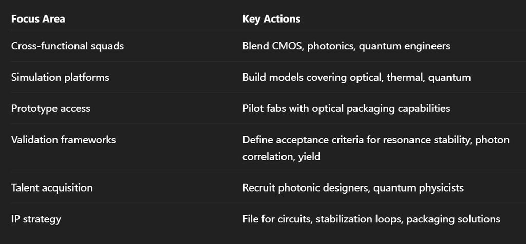
To capitalize on hybrid electronic‑photonic‑quantum technologies, engineering teams must adopt a multidisciplinary approach. First, companies should form cross-functional squads that integrate CMOS designers, photonics experts, and quantum physicists to ensure holistic design capabilities. Simulation platforms must be developed or adapted to accurately model optical, thermal, and quantum behaviors within the same environment. Access to prototype fabrication lines—with photonic packaging capabilities—is critical for early validation. Robust validation frameworks should be established, focusing on performance metrics like resonance stability, photon correlation, and production yield. Recruiting specialized talent in photonics and quantum physics will strengthen internal expertise and accelerate development. Lastly, teams should proactively develop intellectual property strategies, protecting innovations in circuit design, optical stabilization, and advanced packaging methods. These actions collectively enable a strong foundation for building commercially viable, next-generation hybrid chips.
🚀 Closing Thoughts
The emergence of this hybrid electronic‑photonic‑quantum chip marks a paradigm shift. It offers:
A smooth entry point into quantum‑enabled hardware via standard CMOS.
Multiple product pathways—from secure communications to sensors and AI interconnects.
A rich ecosystem and new revenue streams in packaging, tools, and services.
For electronics leaders, now is the moment to map strategic and tactical roadmaps—investing in R&D, forging partnerships, and shaping the chips that will define the next wave of technological innovation.
SERVICES
Peakingtech © 2025. · Shenzhen, China · Privacy Policy · Terms of Service
Contact Form
Metal Parts
Peakingtech® is a registered trademark of Peakingtech Co in the United States.
COMPANY
CONTACT