Breakthrough 3D Chip Technology from MIT Promises Faster, Energy-Efficient Electronics
Discover how MIT’s new monolithic 3D chip stacking method using 2D semiconductors could revolutionize electronic design. Learn the benefits, applications, and strategic implications for engineers and decision-makers in electronics development.
IDEA TO DESIGN
JoeZ
6/19/20255 min read

🚀 Introduction: A Vertical Leap in Semiconductor Design
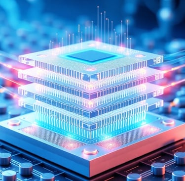
As Moore’s Law decelerates, chipmakers are exploring new horizons for boosting performance and energy efficiency. A promising frontier is vertical integration—stacking chip layers in the Z‑axis instead of shrinking transistors further on a planar surface. MIT researchers have recently unveiled a method to fabricate monolithic 3D chips by stacking high-performance 2D semiconducting layers without intervening silicon wafers—a breakthrough that sidesteps thermal and structural bottlenecks in current 3D processes.
This technique enables denser integration of transistors, memory, and logic circuits while ensuring rapid interlayer communication and compatibility with existing silicon-based fabrication. This article explores the technology’s fundamentals, applications, challenges, and strategic impact for electronics R&D leaders.
1. Background: Why Go Vertical?
1.1 Scaling Limits of Planar Transistors
Moore’s Law has propelled chip scaling, but quantum effects and thermal leakage pose physical limits. Traditional silicon transistors now face breakdown points at the nanoscale .
1.2 The Promise of 3D Integration
3D integration offers:
Footprint reduction: stacking multiple functional layers.
Shorter interconnects: minimizing delays and power by vertical communication.
Heterogeneous integration: combining logic, memory, I/O, RF, photonics, etc., within a single stack.
However, conventional 3D ICs rely on through-silicon vias (TSVs) or wafer bonding that include thick silicon substrates between layers—leading to alignment limits, lower bandwidth, thermal resistance, and manufacturing complexity .
2. MIT’s Innovation: Growth-Based Monolithic 3D
2.1 Core Idea
The MIT team pioneered a growth-based fabrication: they directly grow crystalline 2D semiconductor layers (Transition Metal Dichalcogenides, TMDs) atop each other through low-temperature epitaxy, eliminating intermediary silicon wafers.
Key Steps:
Pattern a thin SiO₂ mask with nanoscale pockets over existing circuits.
Seed TMDs like MoS₂ or WSe₂ along the edges of these pockets.
Grow high-quality single-crystal TMD layers at ~380 °C—crucially low enough to avoid damaging underlying logic.
Repeat layering to stack alternating n-type (MoS₂) and p-type (WSe₂) transistors—building monolithic CMOS stacks.
2.2 Why It Works
Edge-based nucleation from metallurgy enables crystal growth at low temperature (380 °C).
The SiO₂ mask confines the crystal seeds, promoting single-crystal consistency and high film quality abachy.com.
Abrupt interfaces between semiconductor layers result in excellent electrical coupling without thick insulators—a key advantage over TSV‐dependent approaches .
3. Technical Advantages
3.1 Enhanced Density
Doubling the density of semiconducting elements per footprint becomes possible by stacking CMOS layers. This is a major leap over planar scaling and traditional TSV-based 3D ICs.
3.2 Superior Interlayer Communication
Direct adjacency of semiconductor layers results in:
Lower vertical resistance and capacitance
Higher bandwidth communication
Reduced latency, enabling processors and memory to interact faster.
3.3 Energy Efficiency
Stacked logic and memory can utilize short-wire vertical interconnects—lowering energy per operation by an order of magnitude compared to off-chip I/O .
Concurrent MIT projects demonstrate ultralow‑energy 3D photonics, further suggesting long-term gains in efficiency.
3.4 Integration of Logic & Memory
Creating stacks with both transistors and memory layers enables true 3D architectures––ideal for processing-in-memory (PIM) workloads in AI accelerators. Tight vertical coupling boosts both speed and energy performance.
4. Materials & Device Insights
4.1 TMD Choice
MoS₂: high electron mobility for n-type transistors.
WSe₂: p-type TMD for complimentary circuits.
Both exhibit stable semiconducting properties even at atom-thin scales.
4.2 Device Performance
Early devices demonstrated:
Single-crystalline TMD layers achieved at low temperature.
Functional n- and p-type FETs stacked monolithically.
Significant density gains—potentially hundreds of layers stacked.
MIT’s parallel research on 3D nanowire tunneling FETs (GaSb/InAs) hints at sharper switching and lower-voltage operation—ideal for low-power AI applications.
5. Challenges & Open Questions
5.1 Thermal Management
Up to hundreds of active layers will require efficient heat dissipation across vertical paths. Thermal gradients and hotspots could reduce reliability .
5.2 Throughput & Yield
Each stack layer is a potential defect point. Without traditional independent testing and bonding, yield management must adapt to monolithic fabrication models.
5.3 Interconnect Control
While vertical coupling is strong, management of crosstalk and parasitic capacitance between layers needs advanced modeling and layer-level signal integrity strategies.
5.4 Scaling Fabrication
Moving from small-area demonstrators to wafer-scale production implicates:
Advanced thin-film deposition, alignment, and masking.
Compatible steps in existing foundry process flows.
5.5 Design Toolchain & EDA
Monolithic 3D architecture demands:
Synthesis, placement, and routing tools that incorporate vertical dimensions.
Thermal-awareness and 3D signal analysis in timing verification.
Partitioning logic based on 3D layout considerations .
6. Strategic Applications
6.1 AI & Edge Computing
3D-stacked logic and memory layers with low-latency interfaces are ideal for:
On-device neural network inference
PIM architectures that reduce data movement
6.2 Wearables & Mobile Hardware
Thin, vertically integrated chips with efficient heat dispersion and high compute density align well with the needs of wearables and smartphones .
6.3 Data Centers & HPC
By offering supercomputer-level performance in a miniaturized package, these chips could reduce server footprint, power, and cost.
6.4 IoT & Real-Time Systems
Highly integrated logic-memory stacks aid in local processing for autonomous vehicles, robotics, sensor networks, and medical devices .
7. Business & Ecosystem Implications
7.1 IP & Startup Spinout
MIT researchers founded FS2 (Future Semiconductor 2D Materials) to scale this technology for AI chips—signaling early-stage commercial intent.
7.2 Industry Partnerships
Collaborators include Samsung and U.S. Air Force labs—indicative of alignment with both commercial and strategic/government sectors .
7.3 Foundry Adoption
If compatible with current fab thermal budgets (< 400 °C), legacy silicon fabs could incorporate this technology with relatively minor CapEx, expediting industry uptake.
7.4 Roadmapping & Standards
As monolithic 3D gains traction, expect shifts in:
Roadmaps like ITRS/JIC redefining technology nodes vertically .
EDA tools integrating 3D-aware physical and thermal analysis.
Standardizing vertical interfaces and test methodologies.
8. Recommended Roadmap for Electronic Project Leaders
8.1 Initiate Feasibility Studies
Partner with academia (MIT, FS2) to evaluate core device viability: layer quality, crystal integrity, thermal resilience.
Create test chips integrating single-layer logic with memory to quantify latency and energy gains.
8.2 R&D on EDA & Process Flow
Adjust toolchains for 3D placement, routing, and thermal modeling.
Prototype fabrication sequences: seed → grow → pattern → test, iterative across multilayers.
8.3 Application-Targeted Pilots
Identify suitable edge/AI workloads (neural nets, sensor fusion) for pilot design.
Define vertical stack architectures (n logic + m memory + I/O).
8.4 Thermal & Mechanical Modeling
Develop TCAD simulations for thermal dissipation in multilayer structures.
Validate via wafer-level thermal characterization.
8.5 Establish Supply Chain
Engage foundries for compatibility analysis.
Source advanced TMD precursors, mask materials, vapor-deposition tools.
8.6 IP and Standard Development
File patents on layer stack design, seed confinement, vertical coupling techniques.
Collaborate in industry groups to contribute to emerging 3D standards.
9. Future Outlook & Limitations
9.1 Scaling Prospects
Researchers posit tens to hundreds of layers are feasible—translating to orders-of-magnitude improvements in computation density.
9.2 Complementary Advances
Integrating 3D photonics (ultra‑high bandwidth, low‑energy interconnects) would address limitations in horizontal throughput .
9.3 Long-Term Adoption
Broad adoption hinges on:
Overcoming thermal limits, yield challenges.
Embracing new design/test paradigms.
Foundry readiness to retrofit devices into production lines.
If successful, this may herald a new era in:
AI hardware with extremely low-power, high-throughput stacks.
Mobile computing with robust compute in tiny packages.
Data center servers made immensely dense and efficient.
10. Concluding Thoughts
MIT’s novel method for growth-based monolithic 3D stacking of TMDs is a technological watershed. By enabling vertical CMOS layers at low thermal budget, this innovation disrupts the constraints of planar scaling and TSV-reliant 3D ICs.
For engineers and project deciders, it's time to ask:
Which applications benefit most from vertical integration?
Can your current design flow absorb 3D-aware EDA and thermal constraints?
Are existing fab processes capable of TMD growth beneath 400 °C?
How can vertical stacking combine compute, memory, and photonics in your roadmap?
Integration of this technology could redefine architecture, shrinking power, cost, and device size. As FS2 and other partners advance prototyping, teams with the vision to integrate monolithic 3D chips early will be best positioned to lead in next-gen AI, edge, and high-performance electronics space.
References
MIT’s multilayer growth method, temperature thresholds, and seeded crystallization drivingeco.comsciencedaily.com
Single-crystal TMD layering of MoS₂ and WSe₂ for n/p-type CMOS abachy.com
Relationship to broader 3D integration, interconnect, and thermal issues
Energy, bandwidth, and AI implications arxiv.org
Final Thoughts for Leaders
Monolithic 3D stacking may soon transform chip development. It elevates our design horizon from 2D chips approaching physical limits to true 3D compute platforms—dense, efficient, and integrated.
The immediate step is feasibility. Pilot projects should target low-volume AI/edge devices to measure gains. If early results align with MIT's projections, this technology ought to be fast-tracked into product roadmaps—potentially shaping the future of computing architecture.
SERVICES
Peakingtech © 2025. · Shenzhen, China · Privacy Policy · Terms of Service
Contact Form
Metal Parts
Peakingtech® is a registered trademark of Peakingtech Co in the United States.
COMPANY
CONTACT