Beyond the Green: The Ultimate Guide to Transparent PCBs
Get the ultimate guide to Transparent PCBs. Explore the science of clear materials (ITO, glass, nanowires), manufacturing challenges, and revolutionary applications like HUDs and invisible LEDs.
ELECTRONICS MANUFACTURING
JoeZ
11/10/202513 min read
When you picture a "circuit board," what comes to mind?
It’s almost certainly a small, flat sheet of opaque green, blue, or red material, covered in a complex web of tiny, silvery lines and black components. For decades, this has been the unchanging face of electronics. The Printed Circuit Board (PCB) is the unsung hero, the hidden foundation of every device we own, from toasters to supercomputers.
But what if that foundation wasn't hidden? What if it was invisible?
Enter the Transparent PCB. This emerging technology is not just a stylistic gimmick; it’s a fundamental shift in materials science and electronic design, pulling circuits out of the shadows and integrating them directly into the world we see. It’s a technology that allows electronics to merge with glass, plastics, and even the air itself.
This isn't science fiction. Transparent PCBs are already here, powering the touchscreens in your pocket, the "floating" taillights on new cars, and the "smart glass" in modern architecture. But what are they, exactly? How do you make a circuit you can see through? What are the incredible benefits, and what are the daunting challenges?
In this ultimate, 3000-word deep dive, we will pull back the clear curtain. We'll explore the materials, manufacturing processes, applications, and the transparent future of a technology that is, quite literally, changing how we see electronics.
Part 1: What Exactly is a Transparent PCB?
A standard PCB is an inherently opaque object. It's built on a substrate called FR-4, which is a high-pressure laminate of woven fiberglass cloth and a flame-retardant epoxy resin. This combination is strong, cheap, and a great electrical insulator, but it's as see-through as a brick. The circuits on top are made of copper, a very visible, non-transparent metal.
A Transparent PCB, by contrast, is a circuit board designed and manufactured to be optically clear, allowing light to pass through it with minimal distortion.
Achieving this "invisibility" is a two-part challenge. A transparent PCB must solve two fundamental problems:
The Substrate Problem: The opaque FR-4 base must be replaced with a material that is both a good electrical insulator and optically transparent.
The Conductor Problem: The opaque copper traces must be replaced with a conductive material that is also transparent, or so thin that it becomes effectively invisible.
This dual requirement makes transparent PCBs a marvel of material science. They are not one single "thing" but rather a category of solutions that balance trade-offs between clarity, conductivity, cost, and durability.
The "transparency" itself exists on a spectrum. Some boards are "frosted" or "hazy," designed for light diffusion in LED applications. Others, like those used in displays, are "optically clear," rivaling the clarity of a window pane.
The entire goal is to create an electronic circuit that doesn't obstruct a visual path. This simple concept has profound implications, allowing engineers and designers to place electronics in places they were previously impossible: on windows, in eyewear, inside optical lenses, and as aesthetic-first design elements.
Part 2: The Core Components: A Materials Science Deep Dive
The magic of a transparent PCB lies entirely in its materials. Building one requires a completely different "ingredient list" than a traditional board. Let's break down the two main components.
2.1: The Transparent Substrates (The "Board")
This is the mechanical and insulating backbone. Instead of FR-4, engineers must choose from a menu of clear materials, each with its own specific properties.
1. Glass (Soda-Lime, Borosilicate)
Glass is the "gold standard" for optical clarity and stability. It's the obvious first choice when you think "transparent."
Pros:
Exceptional Clarity: Offers the highest level of light transmission.
Thermal Stability: Can withstand high temperatures (especially borosilicate glass), which is a huge advantage during soldering and for high-power components.
Rigidity: Extremely stiff and stable, with no warping.
Chemical Resistance: Very inert and resistant to environmental factors.
Cons:
Brittleness: Glass shatters. It has zero flexibility and is highly susceptible to impact and thermal shock (sudden temperature changes).
Weight: It is significantly heavier than plastic or FR-4.
Machinability: You can't just "drill" glass with a standard PCB drill bit. It requires specialized processes like laser drilling or ultrasonic machining, which are slow and expensive.
Best For: High-end displays, optical sensors, "lab-on-a-chip" medical devices, and harsh-environment applications where clarity is paramount.
2. Polymers (The "Plastics")
Polymers offer a more flexible, durable, and cost-effective alternative to glass. They are the most common choice for large-scale transparent PCBs.
Polycarbonate (PC):
Pros: Incredible impact strength (it's the material used for "bulletproof glass"). Good clarity and easier to machine than glass.
Cons: Softer than glass, meaning it scratches easily. Has a lower thermal stability, which makes soldering a major challenge.
Best For: Durable applications like transparent casings, automotive interiors, and robust handheld devices.
Polyester (PET / PETG):
Pros: Flexible! This is the key property. PET can be used to create flexible transparent circuits. It's also very low-cost and widely available.
Cons: Very poor thermal resistance. It will warp and melt at standard soldering temperatures. It can also turn yellow over time with UV exposure.
Best For: The number one application for PET is LED lighting strips. It's also used in disposable medical sensors and simple flexible displays.
PMMA (Acrylic):
Pros: Better optical clarity than polycarbonate and is very scratch-resistant (compared to other plastics).
Cons: More brittle than PC (though much less than glass). Poor thermal properties.
Best For: Aesthetic-focused applications, decorative panels, and light-guide panels.
Polyimide (PI):
Pros: A high-performance polymer. It has fantastic thermal stability (it can be soldered on) and good mechanical properties.
Cons: Traditional polyimide is naturally an amber/yellow color. Truly transparent polyimides exist, but they are specialized, expensive, and a major focus of current research.
Best For: Flexible circuits that need to withstand high temperatures, such as in aerospace or advanced wearable devices.
2.2: The Transparent Conductive Materials (The "Traces")
This is where the real challenge lies. How do you make something that conducts electricity—a property of metals—but is also see-through?
1. Indium Tin Oxide (ITO)
ITO is the established incumbent and the most common Transparent Conductive Material (TCM) in the world. You are almost certainly touching an ITO-based circuit right now—it's the material used to make the capacitive touch layer on your smartphone screen.
What it is: A ceramic composed of indium oxide and tin oxide. It's deposited on a substrate (like glass or PET) in a very thin layer (a few nanometers thick) using a process called sputtering.
Pros: Excellent optical transparency (up to 90%) combined with good electrical conductivity (for a transparent material).
Cons:
Cost & Scarcity: Indium is a rare-earth element, making ITO expensive and subject to price volatility.
Brittleness: As a ceramic, ITO is very brittle. It cracks when flexed, making it a poor choice for flexible applications (though it's used on a "flex-to-install" basis).
Resistivity: It is far more resistive than copper. This means it cannot handle high currents and is limited to low-power applications (signals, touch sensing, LEDs).
2. Silver Nanowires (AgNWs)
This is the leading "challenger" to ITO, especially for flexible electronics.
What it is: Instead of a solid film, AgNWs are a "mesh" or "percolated network" of microscopic silver wires suspended in a liquid ink. This ink is coated onto the transparent substrate. The wires are so small (nanometers in diameter) that they are individually invisible, but they overlap enough to create a conductive path.
Pros:
Flexibility: The mesh can be bent, folded, and stretched without breaking the conductive path. This is its killer feature.
Conductivity: Offers better conductivity (lower resistance) than ITO.
Cost: Silver is cheaper and more abundant than indium. The ink-based "printing" process can be cheaper than ITO sputtering.
Cons:
Haze: The random network of wires can scatter light, creating a slight "haze" that can be undesirable in high-clarity displays.
Stability: The nanowires can be susceptible to oxidation (corrosion) over time, which can degrade performance.
3. Other "Future" Materials
This is an active area of R&D, with several "wonder materials" vying for the top spot.
Carbon Nanotubes (CNTs): Similar to AgNWs, these are microscopic tubes of carbon that can be made into a conductive, transparent, and flexible film. They are extremely strong and chemically stable, but controlling their conductivity and purifying them is still a major manufacturing hurdle.
Graphene: The "ultimate" material. A one-atom-thick sheet of carbon that is theoretically perfectly transparent, more conductive than copper, stronger than steel, and perfectly flexible. The challenge? Manufacturing a perfect, large-scale sheet of graphene is currently prohibitively difficult and expensive.
4. The "Cheat" Method: Ultra-Fine Copper Traces
Sometimes, the best solution is the simplest. For many applications, especially in LED lighting, the circuit doesn't need to be truly transparent. It just needs to appear transparent.
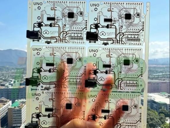
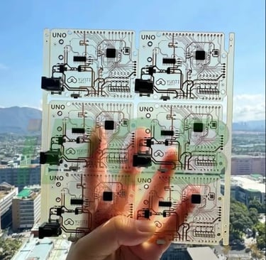
This is achieved by using a standard transparent substrate (like PET or PC) and fabricating copper traces that are extremely thin (e.loc, < 25-50 micrometers wide). From a normal viewing distance, these "micro-wires" are so fine that they are effectively invisible, giving the illusion of a perfectly clear board. This method has the huge advantage of using copper, which means it can handle much-higher currents and can be manufactured using more traditional (and cheaper) etching processes.
Part 3: How Are Transparent PCBs Made?
You can't manufacture a transparent PCB using the same old FR-4 process. The unique materials demand unique fabrication techniques, which are often more complex and delicate.
Method 1: Subtractive Etching (For ITO & Fine-Line Copper)
This process is most similar to traditional PCB manufacturing.
Start with Coated Substrate: You don't start with a bare piece of glass. You start with a "pre-coated" substrate, such as a sheet of glass or PET that already has a thin, uniform layer of ITO or a thin copper foil laminated on top.
Apply Photoresist: A light-sensitive chemical (photoresist) is coated over the entire conductive layer.
Expose: A "phototool" (a mask with the circuit pattern) is placed over the board. The board is then exposed to UV light. The light "hardens" the photoresist in the pattern of the desired traces.
Develop: The board is washed in a chemical bath that removes the unhardened photoresist, leaving the conductive layer exposed except for the areas that will become traces.
Etch: The board is placed in a much stronger chemical bath (a specific acid for ITO, a different one for copper) that "etches" away all the exposed conductive material. Only the hardened-photoresist-protected traces remain.
Strip: The final photoresist "cap" is chemically stripped away, leaving behind the finished transparent circuit on its clear substrate.
Method 2: Additive Printing (For AgNWs & Conductive Inks)
This is a more futuristic and often more efficient method, similar to inkjet printing.
Start with Bare Substrate: You begin with a simple, clean sheet of transparent glass or polymer.
Direct Printing: A high-precision printer (using techniques like screen printing, inkjet printing, or slot-die coating) deposits the special conductive ink (e.g., silver nanowire ink) only where the traces need to be. There is no etching and no wasted material.
Curing/Sintering: The printed "wet" traces must be "cured" to become solid and conductive. This is a critical step.
Thermal Curing: The board is baked in an oven. This is fine for glass, but a major problem for low-temperature plastics like PET, which can warp.
UV Curing: The ink contains a UV-sensitive binder, and it's hardened with UV light.
Photonic Sintering: A very new technique that uses a high-intensity, millisecond-long pulse of light. This "flash-welds" the conductive particles together instantly without heating the underlying (and delicate) plastic substrate.
The Overlooked Hurdle: Soldering and Assembly
This is, by far, the biggest manufacturing challenge for transparent PCBs.
Problem 1: The Heat. Standard solder (SAC305) melts at around 217°C (423°F), and soldering irons run at 260°C (500°F) or higher.
PET and Polycarbonate will instantly melt, warp, and deform at these temperatures.
Glass can handle the heat, but the rapid, localized temperature change from a soldering iron can cause a thermal shock, cracking the entire board.
Problem 2: The Traces.
ITO and AgNWs are delicate. They are thin-film deposits, not bulk metal. Touching them with a hot soldering iron can "burn" them, destroying their conductivity or causing them to delaminate from the substrate.
The Solutions:
Low-Temperature Solders: This is the most common solution. Engineers use special solder alloys, often based on Bismuth or Indium, that melt at much lower temperatures (e.g., 138°C or 158°C). This is "hot" enough to melt the solder but "cool" enough to not destroy the plastic substrate.
Conductive Epoxies: Instead of solder, components are literally glued to the board using a two-part epoxy that is infused with silver particles. When the epoxy cures, it forms a strong, conductive bond. This is a very common technique in high-end, delicate electronics.
Specialized Connectors: Designing the board to use Zero Insertion Force (ZIF) connectors or pressure-based "pogo pin" connections, avoiding soldering altogether.
Part 4: The Good, The Bad, and The Clear (Pros & Cons)
Transparent PCBs are not a "replacement" for FR-4. They are a specialized solution with a unique set of trade-offs.
✅ Advantages (The "Good")
Aesthetics and Design: This is the most obvious benefit. Electronics can be made "invisible" or can be celebrated as a "floating" design element. This allows for minimalist, futuristic products that were previously impossible.
Optical Integration: This is the most powerful technical advantage. A transparent PCB can be placed directly in an optical path. You can mount sensors, light emitters (LEDs, lasers), and detectors on a board that is also a lens, a window, or part of a camera assembly.
Miniaturization and Dual-Function: A transparent PCB can serve two purposes at once. A car's windshield can be the circuit board for a heads-up display. A wearable sensor can be the clear "skin" of the device. This saves space and reduces component count.
Unique Form Factors: The use of polymer substrates allows for transparent circuits that are also rigid, flexible, or even stretchable, opening up new possibilities for wearable tech and integrated surfaces.
❌ Disadvantages (The "Bad" & The Challenging)
Cost: This is the biggest barrier. Exotic materials (Indium, AgNWs, optical-grade polymers) and complex, delicate manufacturing processes (sputtering, laser drilling, low-temp assembly) make transparent PCBs significantly more expensive than mass-produced FR-4 boards.
Electrical Performance Limitations: This is the key technical limitation. Transparent conductors are not as good as copper. They have higher resistance, which means:
They cannot handle high currents (no power-hungry motors or high-wattage devices).
They perform poorly at high frequencies (limiting their use in Wi-Fi, 5G, or high-speed data processing).
They are best suited for low-power applications: LEDs, sensors, touchscreens, and simple logic circuits.
Thermal Management: This is a critical failure point. Polymers like PET and PC are thermal insulators (they trap heat). FR-4 is not great, but copper planes in a traditional PCB are excellent at spreading and dissipating heat. On a transparent board, heat-generating components (like a CPU or even an LED) have nowhere to send their thermal energy, leading to rapid overheating and failure.
Durability and Robustness: Glass is brittle. Polymers scratch easily and can be sensitive to UV light and chemicals. The conductive traces themselves are delicate. Transparent PCBs are not, as a rule, "rugged" devices.
Part 5: Real-World Applications (Where You Can Find Them)
This technology is already more common than you think. Its applications are growing as the cost comes down and the technology improves.
1. LED Lighting (The #1 Application)
This is the "killer app" for transparent PCBs today, particularly the flexible PET + fine-copper-trace variant. By mounting LEDs on a clear, flexible strip, designers can create "floating" lights, lights that curve around architectural elements, and "invisible" light sources that are only seen when turned on.
Examples: Automotive taillights and daytime running lights, architectural cove lighting, retail and museum display lighting, decorative "filament" bulbs.
2. Displays and Touchscreens
This is the most widespread (and most overlooked) application.
Touchscreens: Your phone's capacitive touch panel is a complex grid of transparent ITO traces on a glass substrate. It's a transparent circuit that sits on top of the display, sensing your finger.
Transparent Displays: True see-through displays (as seen in sci-fi films) are an emerging market. They use technologies like micro-LEDs or OLEDs mounted on a fully transparent glass substrate, allowing you to see the display and the world behind it.
Examples: Smartphone screens, high-end retail displays, smart-watch faces.
3. Automotive and Aerospace
This is a huge growth area, driven by the need to integrate data into the driver's or pilot's line of sight.
Heads-Up Displays (HUDs): A transparent circuit (often a transparent heater to defog) is laminated directly into the car's windshield. Information is then projected onto this layer, making it appear to "float" over the road.
Smart Glass: Transparent circuits are used as the electrodes for "smart glass" (PDLC or electrochromic glass) that can tint at the push of a button. This is used in high-end cars (sunroofs) and in the windows of the Boeing 787 Dreamliner.
Examples: HUDs, "smart-tinting" sunroofs, illuminated dashboards.
4. Medical Devices
Clarity and disposability are key advantages in the medical field.
"Lab-on-a-Chip" (Microfluidics): A transparent glass PCB can have micro-channels etched into it for analyzing blood samples. The transparent circuit traces can act as heaters to control the reaction, or as sensors to detect a biological agent, all while the sample is being viewed under a microscope.
Wearable Sensors: Transparent, flexible sensors (using AgNWs) can be applied to the skin like a temporary tattoo to monitor heart rate (ECG) or blood-oxygen levels without being visually obtrusive.
Examples: Diagnostic slides, transparent X-ray detectors, "invisible" patient monitors.
5. Consumer Electronics and Aesthetics
For some products, the "wow" factor is the entire point.
"See-Through" Devices: The dream of a fully transparent phone or laptop is a recurring design concept. While fully transparent CPUs or batteries don't exist, the circuit boards connecting the components can be.
Minimalist Design: Using a transparent PCB as the main structural element of a device, like a smartwatch or a smart speaker, where the "glowing" or "floating" components are the entire aesthetic.
Examples: "Nothing" brand phones (which use transparency as a key design motif), transparent touchpads, high-end audio equipment.
Part 6: The Future of "Invisible" Electronics
The Transparent PCB is just the beginning. The research being done in this field is pushing the boundaries of what's possible, moving from merely "transparent" to truly integrated.
Improved Materials: The hunt is on for the "perfect" transparent conductor—a material with the conductivity of copper, the transparency of glass, the flexibility of rubber, and the cost of plastic. Graphene and new metal-mesh formulations are the top contenders.
3D Additive Manufacturing: Why stay 2D? Researchers are using multi-material 3D printers to print a single, solid object that contains a rigid transparent casing, flexible internal gaskets, and conductive transparent traces, all in one "print job." This is the future of fully integrated device manufacturing.
Stretchable and Biocompatible: Moving beyond "flexible" (bendable) to "stretchable" (like rubber). These circuits, based on AgNWs in a stretchable silicone-like substrate, can be integrated directly into clothing or even used for medical implants that move with the human body.
AR/VR Integration: The single biggest driver for this technology will be Augmented and Virtual Reality. Every pair of "smart glasses" needs a "smart lens." That lens must be a transparent PCB, capable of both displaying data (micro-LEDs) and "seeing" the world (image sensors) on a single, clear, optical-grade element.
Conclusion: A Clear Vision for the Future
The humble green circuit board isn't going away. For the vast majority of electronics—the "guts" of your PC, your washing machine, or your car's engine controller—FR-4 and copper remain the undefeated champions of cost, power, and reliability.
But that's no longer the only story.
The Transparent PCB represents a paradigm shift. It's the evolution of electronics from being a "hidden component" to being an "integrated feature." It's a new design language, a new set of tools, and a new way of thinking about the objects we build.
It's a technology that bridges the gap between the digital and the physical, between the circuit and the surface, between the logic and the light. The challenges of cost, power, and heat are still very real, but the applications are too compelling to ignore.
The next time you see a "floating" light, touch a smart-glass window, or see data projected onto a windshield, you'll know the secret: a complex, high-tech, and beautifully engineered circuit that has learned how to get out of its own way.
The future of electronics isn't just faster or smaller. It's also becoming, quite clearly, invisible.
SERVICES
Peakingtech © 2025. · Shenzhen, China · Privacy Policy · Terms of Service
Contact Form
Metal Parts
Peakingtech® is a registered trademark of Peakingtech Co in the United States.
COMPANY
CONTACT